

Highly reliable optical waveguide device
- Summary
- Abstract
- Description
- Claims
- Application Information
AI Technical Summary
Benefits of technology
Problems solved by technology
Method used
Image

Examples
Embodiment Construction
[0042] Best modes of carrying out the present invention will be described in further detail using various embodiments with references to the accompanying drawings.
[0043] Next, details explain the embodiments regarding implementation aspects.
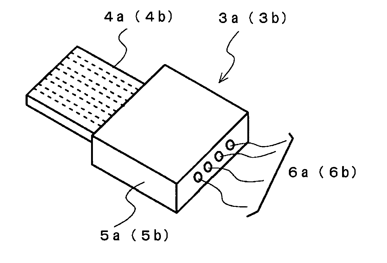
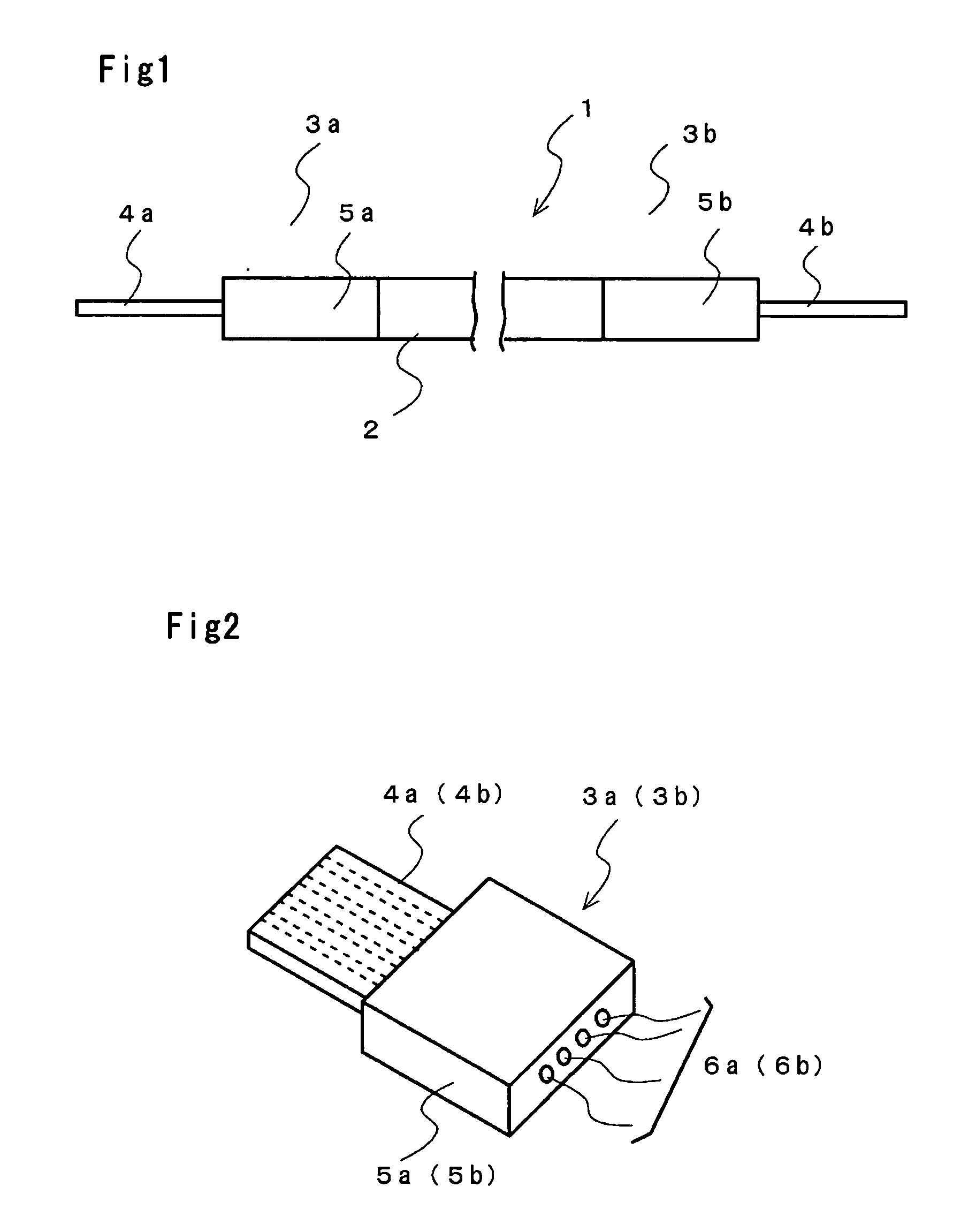
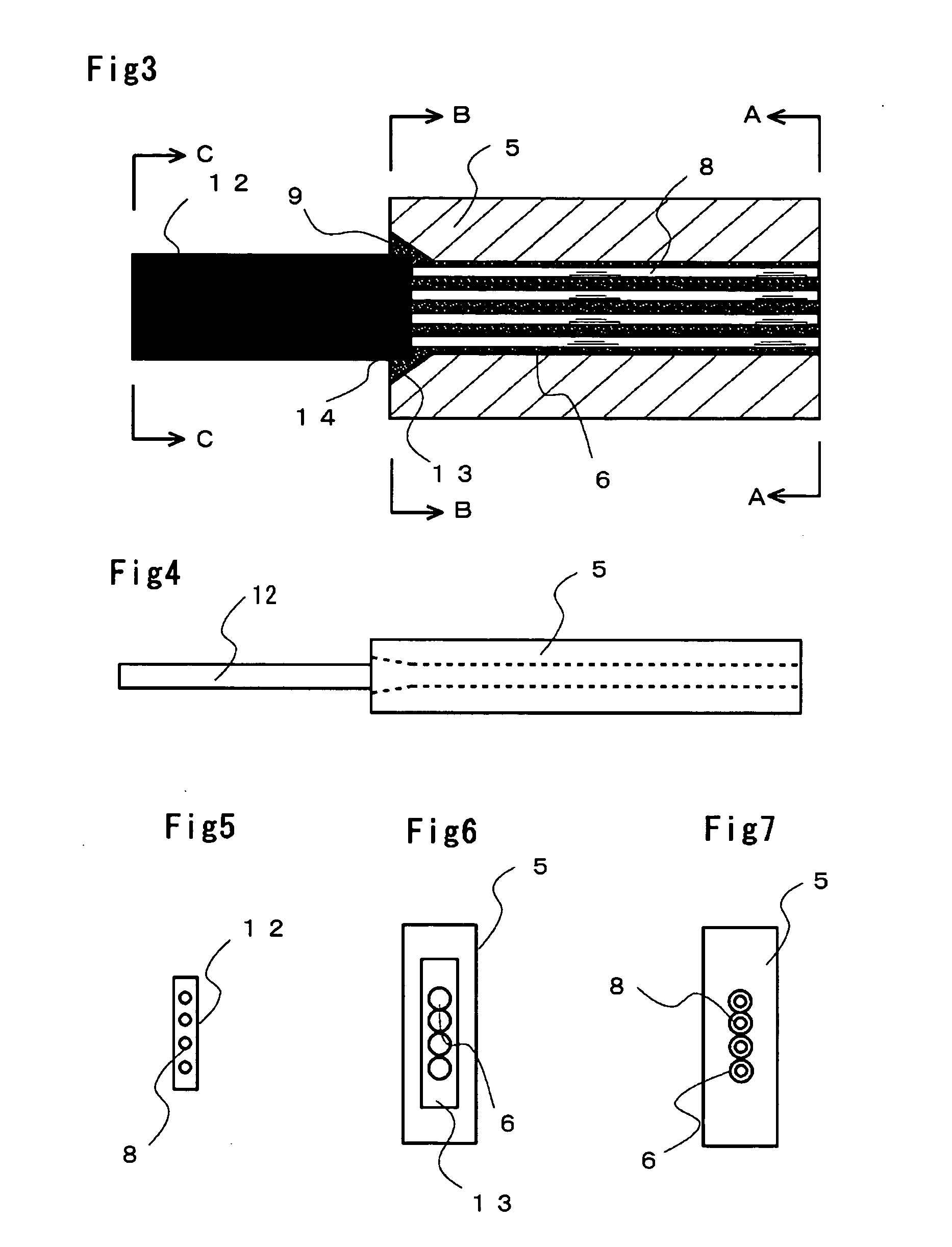
[0044]FIG. 1 is a plan view of an optical waveguide device according to the present invention.
[0045] In FIG. 1, an optical waveguide device 1 according to the present invention comprises a waveguide chip and an optical fiber array connected to each other. According to the embodiment, an optical fiber array 3a and an optical fiber array 3b are connected to both ends of a waveguide chip 2. The optical fiber array 3a comprises an optical fiber 4a and an optical fiber holding member 5a. The optical fiber array 3b comprises an optical fiber 4b and an optical fiber holding member 5b. The waveguide chip 2 comprises a waveguide splitter, an optical switch, or a variable optical attenuator, for example. Any of the waveguide chips is selected for use in...
PUM
 Abstract
Description
Claims
Application Information