Plasma display device

a technology of plasma and display device, which is applied in the direction of discharge tube main electrodes, electrical apparatus construction details, incadescent cooling arrangements, etc., can solve the problems of deterioration of the quality image, large amount of heat generated by pdp, and overall brightness of pdp, so as to enhance heat removal efficiency and improve structure

Inactive Publication Date: 2005-01-27
SAMSUNG SDI CO LTD
View PDF19 Cites 14 Cited by
  • Summary
  • Abstract
  • Description
  • Claims
  • Application Information

AI Technical Summary

Benefits of technology

[0014] The present invention provides a plasma display device having an improved structure so as to enhance heat removal efficiency.

Problems solved by technology

The plasma display devices having the above-described structure display an image using a discharge phenomenon, which causes the PDP to generate a large amount of heat.
A solution for the non-uniform heat distribution has not been suggested, which results in a deterioration of the quality image.
As a result, the overall brightness of the PDP deteriorates.
Also, a failure to eliminate temperature deviations on the PDP causes heat stress, which can cause the glass of the PDP to crack.
The chassis base can have an uneven portion due to the manufacture limitations.
When the air gap is not removed during bonding of the PDP to the chassis base, the air gap reduces heat removal efficiency.
Since the entire surface of the PDP adheres to the entire surface of the chassis base, an air gap is highly likely to be formed.
Also, a discharge path for air is not secured during pressure bonding, and thus the air gap can remain.
Moreover, since heat generated by the PDP is mainly transmitted to the chassis base, the circuit portion on the chassis base can deteriorate.

Method used


Image

  • Plasma display device
  • Plasma display device
  • Plasma display device

Examples


Embodiment Construction

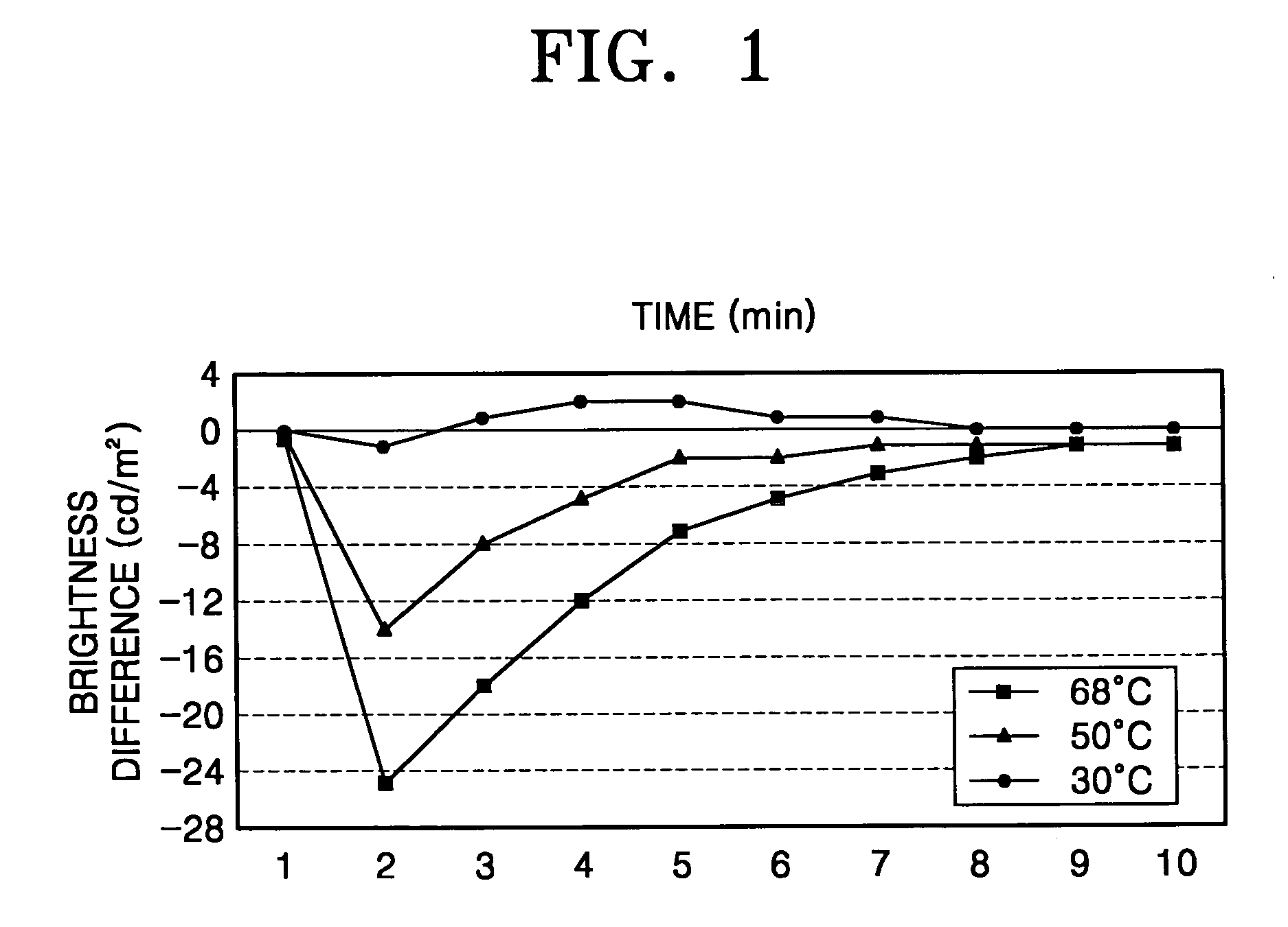
[0054]FIG. 1 is a profile of brightness differences depending on a temperature of a PDP. As shown in FIG. 1, as the temperature of the PDP increases, the brightness difference between the discharge cell in which the relatively large amount of heat has accumulated and a discharge cell in which heat has not accumulated increases.

[0055] Hereinafter, exemplary embodiments of the present invention will be described in detail with reference to the attached drawings.

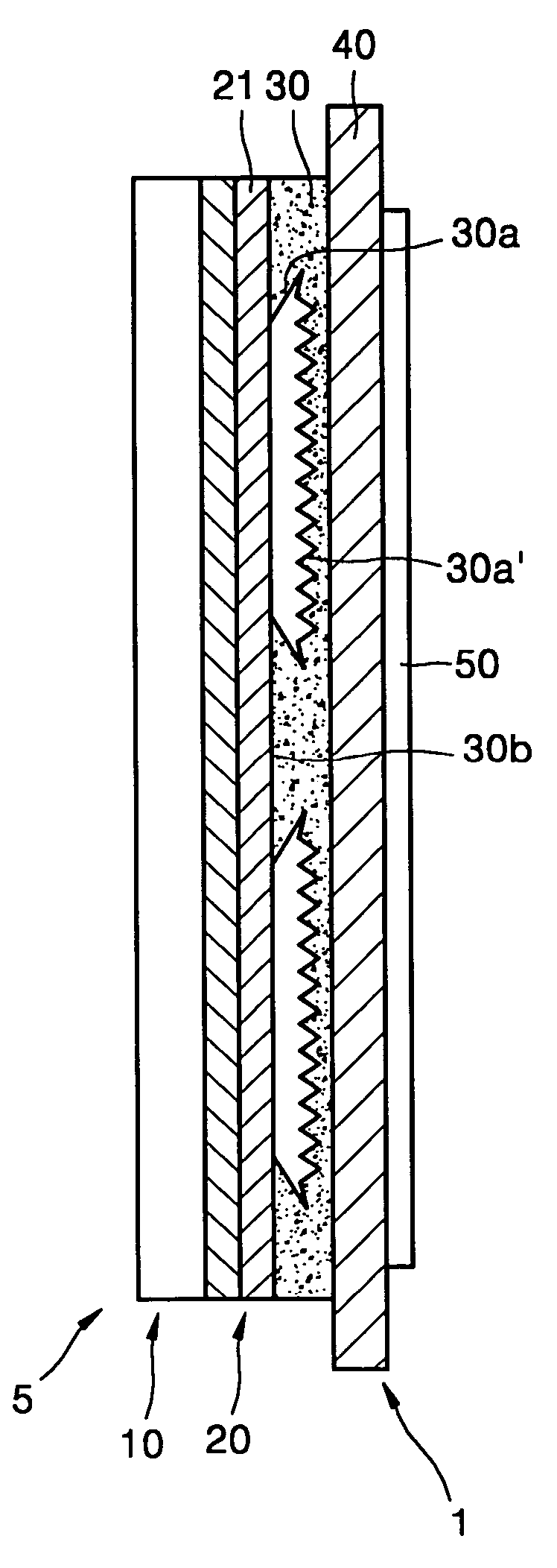
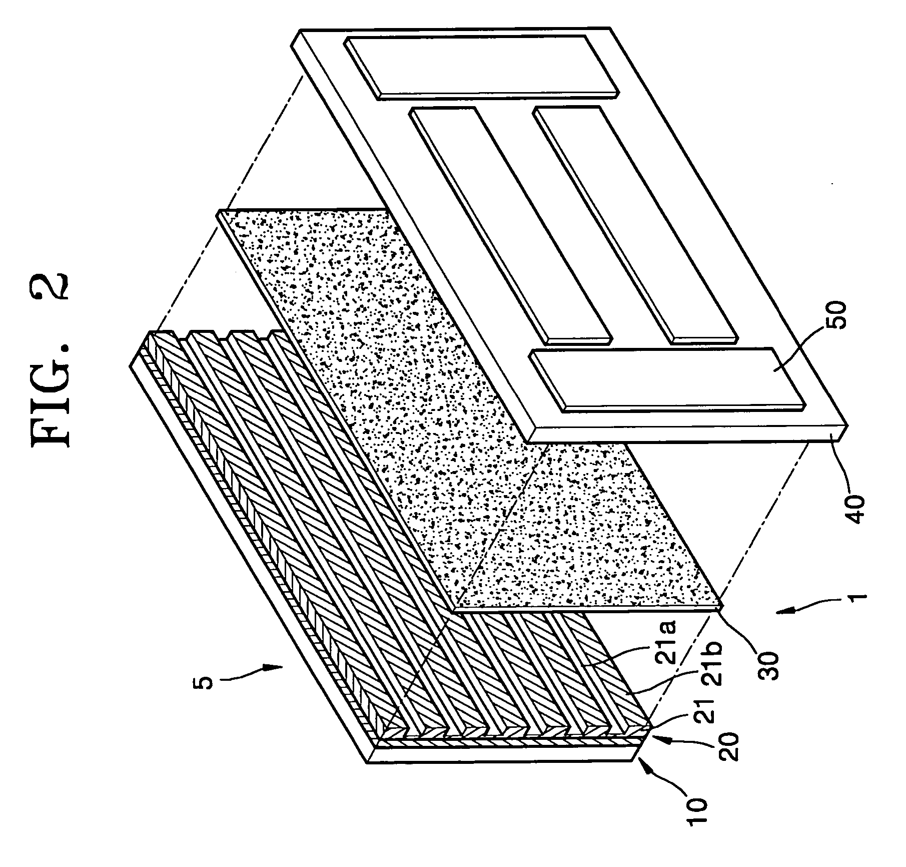
[0056]FIG. 2 is an exploded perspective view of a plasma display device, according to an embodiment of the present invention. Referring to FIG. 2, a plasma display device 1 includes a PDP 5, a chassis base 40, and a circuit portion 50. A heat dissipating sheet 30 can be interposed between the PDP 5 and the chassis base 40.

[0057] The chassis base 40 includes uneven portions, such as bosses 40d of FIG. 10, or holes (not shown) through which wires pass, so that the circuit portion 50 is installed on a rear surface of the chassi...


PUM


Abstract

A plasma display device includes a plasma display panel having a front substrate and a rear substrate spaced apart from the front substrate to form a plurality of discharge spaces, and a chassis base facing the plasma display panel. The plasma display device includes at least one channel adapted to allow air to flow therethrough to improve heat removal efficiency, the at least one channel being arranged between the rear substrate and the chassis base.

Description

CLAIM OF PRIORITY [0001] This application makes reference to, incorporates the same herein, and claims all benefits accruing under 35 U.S.C. § 119 from an application for PLASMA DISPLAY DEVICE earlier filed in the Korean Intellectual Property Office on Jul. 22, 2003 and there duly assigned Serial No. 2003-50340. BACKGROUND OF THE INVENTION [0002] 1. Field of the Invention [0003] The present invention relates to a plasma display device, and more particularly, to a plasma display device including a channel to improve heat removal efficiency. [0004] 2. Description of the Related Art [0005] Plasma display devices generally display an image using a discharge phenomenon and have high-quality display capacity, such as the number of displayable colors, brightness, contrast, afterimage, viewing angle, and the like. Since the plasma display devices are thin and enable large screen displays, they have come into the spotlight as devices capable of replacing CRTs. [0006] Such a plasma display de...

Claims


Application Information

Patent Timeline
Patent Type & Authority Applications(United States)
IPC IPC(8): H01J17/28H01J17/49H05K7/20
CPCH01J11/12H01J11/34H05K7/20972H05K7/20963H01J2211/66H01J11/10H01J17/16H01J17/28
Inventor KIM, WOO-TAE
Owner SAMSUNG SDI CO LTD
Why Eureka
Try Eureka