Method of fabricating a microelectronic die

a technology of microelectronic dies and dies, applied in the direction of basic electric elements, electrical equipment, semiconductor devices, etc., can solve the problem of relatively limited stress that can be provided by these processes

Inactive Publication Date: 2005-01-27
INTEL CORP
View PDF10 Cites 18 Cited by
  • Summary
  • Abstract
  • Description
  • Claims
  • Application Information

AI Technical Summary

Problems solved by technology

The degree of stress that can be provided by these processes is usually relatively limited, which, when making a C-MOS

Method used


Image

  • Method of fabricating a microelectronic die
  • Method of fabricating a microelectronic die
  • Method of fabricating a microelectronic die

Examples


Embodiment Construction

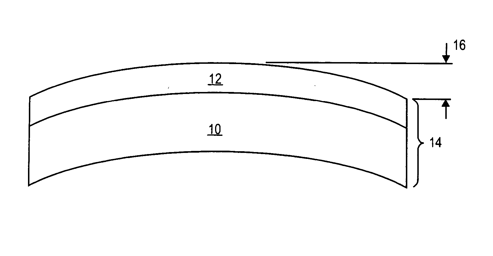
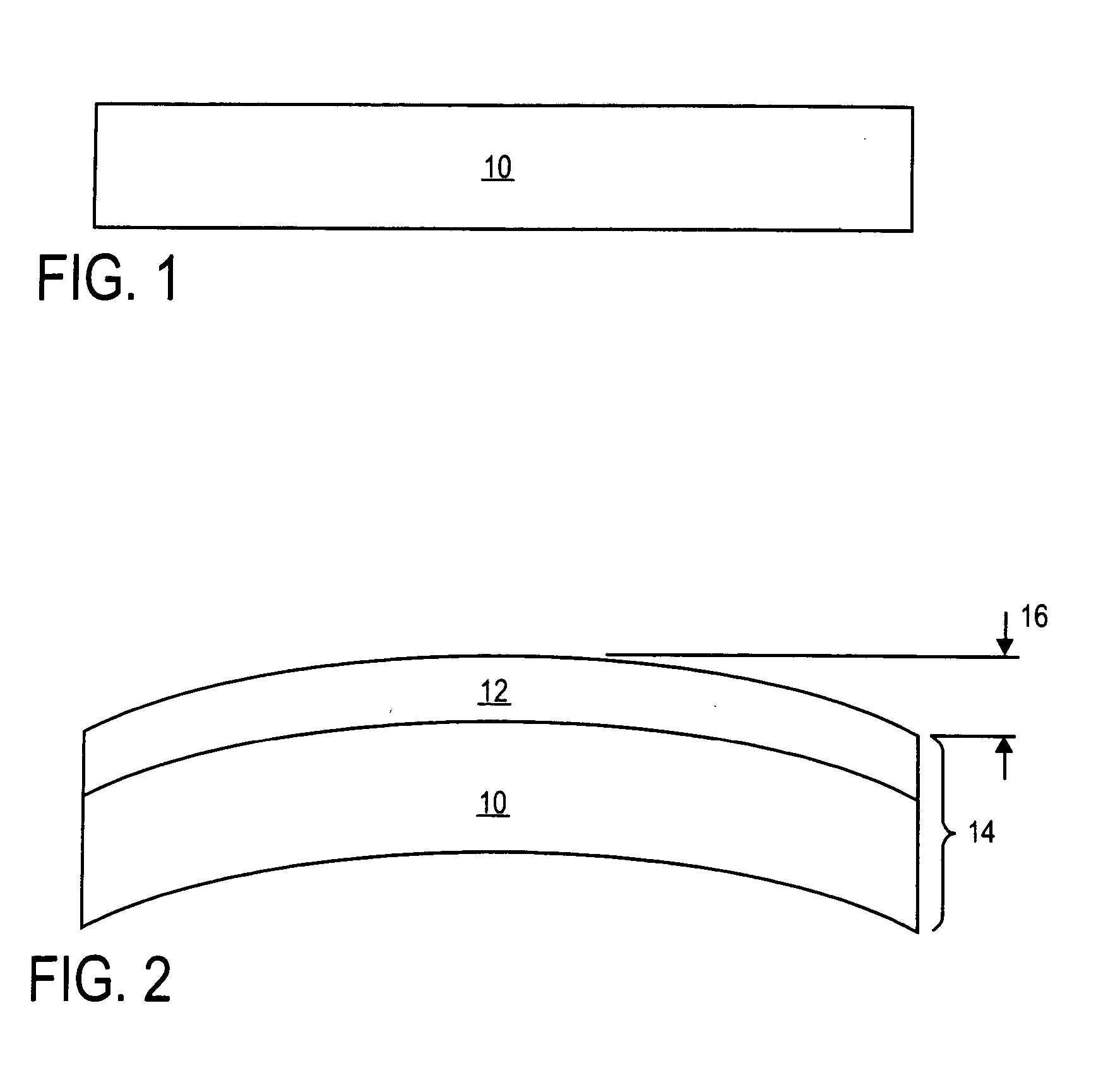
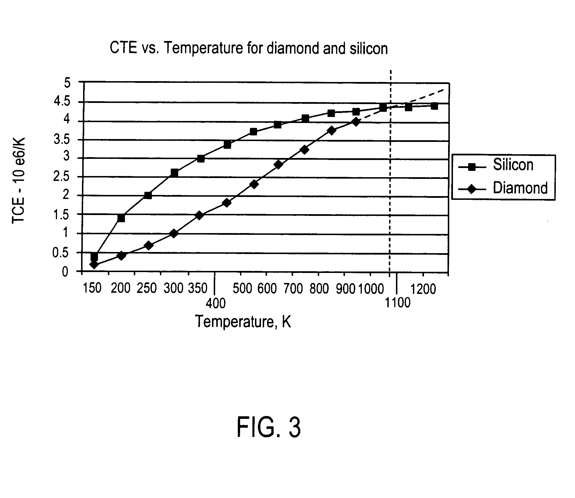
[0017] A method of fabricating a microelectronic die is provided. Transistors are formed in and on a semiconductor layer. A channel of each transistor is stressed after the transistors are manufactured by first forming a diamond intermediate substrate at an elevated temperature on a handle substrate, allowing the intermediate substrate and the handle substrate to cool, attaching the semiconductor layer, and then removing the handle substrate. The intermediate substrate has a lower CTE than the handle substrate, so that the intermediate substrate tends to bow when the handle substrate is removed. Such bowing creates a tensile stress, which translates into a biaxial strain in channel regions of the transistors. Excessive bowing is counteracted with a compensating polysilicon layer formed at an elevated temperature and having a higher CTE on a side of the diamond intermediate substrate.

[0018] As illustrated in FIG. 1, the method of fabricating a microelectronic die, according to an em...


PUM


Abstract

A method of fabricating a microelectronic die is provided. Transistors are formed in and on a semiconductor substrate. A channel of each transistor is stressed after the transistors are manufactured by first forming a diamond intermediate substrate at an elevated temperature on a handle substrate, allowing the intermediate substrate and the handle substrate to cool, and then removing the handle substrate. The intermediate substrate has a lower coefficient of thermal expansion than the handle substrate, so that the intermediate substrate tends to bow when the handle substrate is removed. Such bowing creates a tensile stress, which translates into a biaxial strain in channels of the transistors. Excessive bowing is counteracted with a compensating polysilicon layer formed at an elevated temperature and having a higher CTE on a side of the diamond intermediate substrate.

Description

BACKGROUND OF THE INVENTION [0001] 1. Field of the Invention [0002] This invention relates generally to a method of fabricating a microelectronic die, and more specifically to a method for increasing electron mobility values of channel regions of semiconductor transistors. [0003] 2. Discussion of Related Art [0004] Transistors that make up integrated circuits of microelectronic dies are manufactured in and on silicon or other semiconductor substrates. Such a transistor has a channel region and source and drain regions on opposing sides of the channel region. The transistor further has a gate dielectric layer and a gate electrode which are formed on the channel region. A voltage that switches on the gate electrode can switch a current that flows between the source and drain regions through the channel region. [0005] It has been recognized that a large tensile stress can increase both electron mobility of N-MOS devices and hole mobility of P-MOS devices. Several approaches to inducing...

Claims


Application Information

Patent Timeline
IPC IPC(8): H01L21/20H01L29/78
CPCH01L21/2007H01L29/7842H01L29/78
Inventor RAVI, KRAMADHATI V.
Owner INTEL CORP
Why Eureka
Try Eureka