Probe for combined signals

a combined signal and probe technology, applied in the direction of measurement devices, semiconductor/solid-state device testing/measurement, instruments, etc., can solve the problems of unsuitable higher-frequency unsuitable use of probing assemblies of the type just described, and difficulty in using typical microwave probes

Inactive Publication Date: 2005-02-03
CASCADE MICROTECH
View PDF8 Cites 106 Cited by
  • Summary
  • Abstract
  • Description
  • Claims
  • Application Information

AI Technical Summary

Problems solved by technology

This type of probing assembly, however, is unsuitable for use at higher frequencies, including microwave frequencies in the gigahertz range, because at such frequencies the needle-like tips act as inductive elements and because there are no adjoining elements present to suitably counteract this inductance with a capacitive effect in a manner that would create a broadband characteristic of more or less resistive effect.
Accordingly, a probing assembly of the type just described is unsuitable for use at microwave frequencies due to the high levels of signal reflection and substantial inductive losses that occur at the needle-like probe tips.
However, when testing certain devices, such as laser diodes, the use of a typical microwave probe is problematic.
As a result, there is a significant impedance mismatch with

Method used


Image

  • Probe for combined signals
  • Probe for combined signals
  • Probe for combined signals

Examples


second embodiment

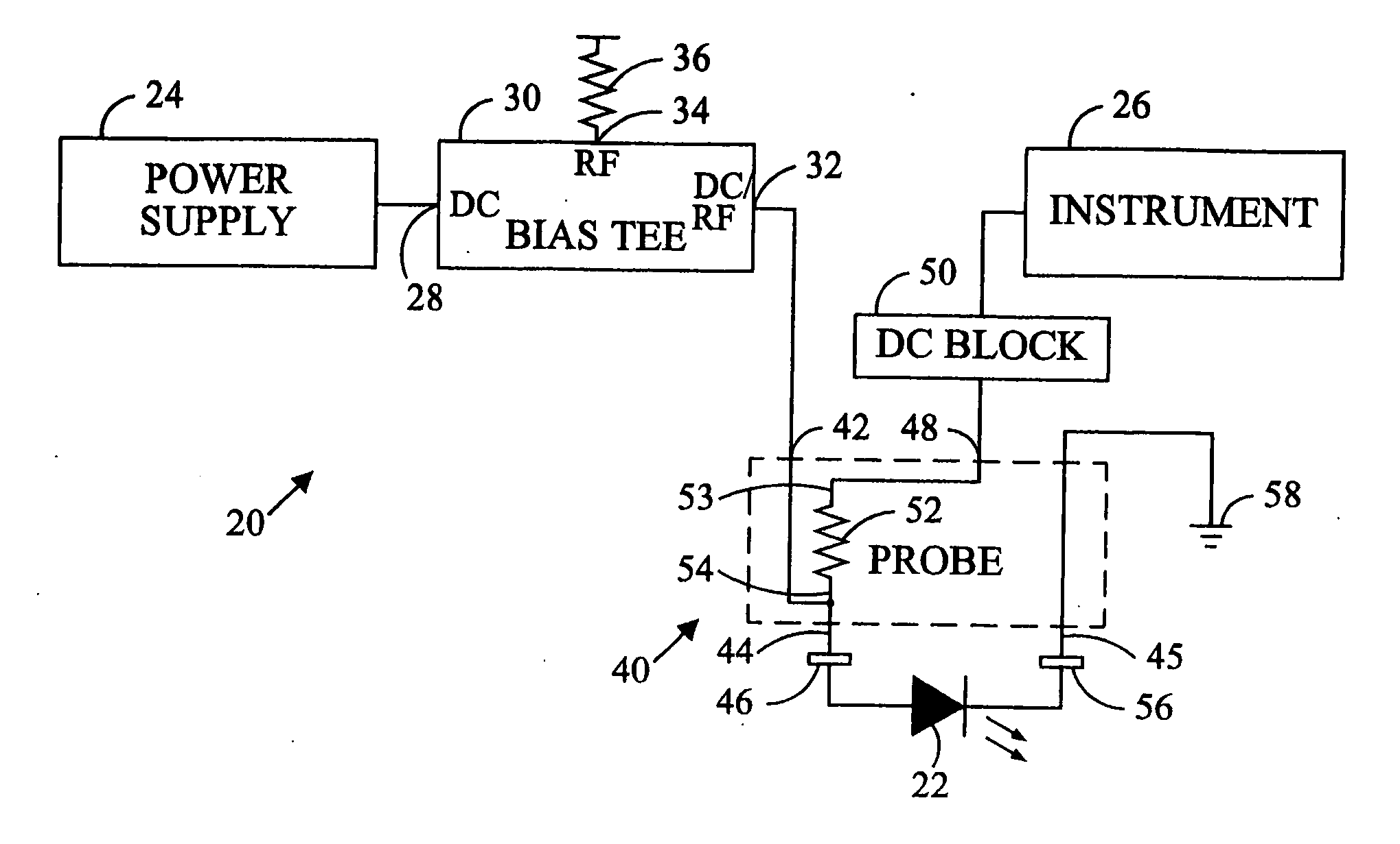
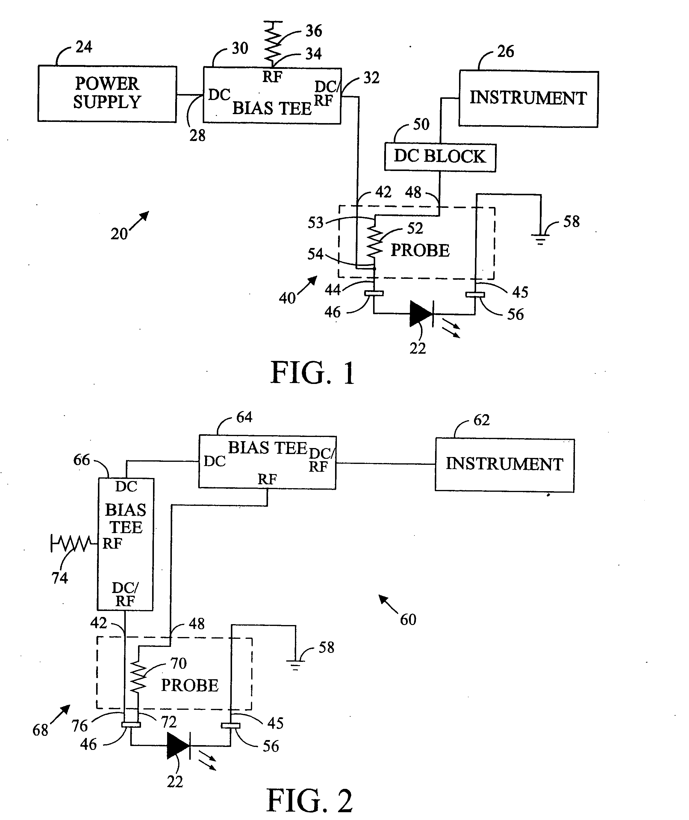
[0024] Referring to FIG. 2, in the probing system 60, the instrumentation 62 is the source of an offset modulation signal. The combined DC current and modulation signal are transmitted to a combined signal port of a first bias tee 64. In the first bias tee 64, the DC current and modulation signal components are separated. The modulation signal is transmitted to the first input port 48 of the combined signal probe 68 which is conductively connected to the first port of an impedance matching resistor 70. The second port of the impedance matching resistor 70 of the probe 68 is connected to a modulation signal contact tip 72 arranged to selectively engage the signal contact pad 46 of the DUT 22.

first embodiment

[0025] The DC current is transmitted from the first bias tee 64 to a second bias tee 66. The combined signal (DC / RF) port of the second bias tee 66 is connected to the second input port of the probe 42 which is conductively connected to a DC signal probe 76 arranged to engage the signal contact pad 46 of the DUT 22 when the modulation signal probe 72 is in engagement with the signal contact pad. An impedance matched termination for the modulation signal imposed on the conductor connecting the second bias tee 66 to the DC signal probe 76 is provided by a termination resistor 74 connected to the RF port of the second bias tee 66. As in the first embodiment, the modulation signal is applied to the signal contact pad 46 of the DUT 22 over a distortion minimizing impedance matched signal path while the DC current is simultaneously applied to the signal contact pad over a signal path that does not include the impedance matching resistor and, therefore, minimizes power dissipation.

[0026] R...


PUM


Abstract

A direct current and a modulation signal are simultaneously applied to contact pads on a device under test, such as a laser diode. A probe and method of probing reduces signal distortion and power dissipation by transmitting a modulated signal to the device-under-test through an impedance matching resistor and transmitting of a direct current to the device-under-test over a second signal path that avoids the impedance matching resistor.

Description

CROSS-REFERENCE TO RELATED APPLICATIONS [0001] This is a continuation of application Ser. No. 10 / 712,579 which is a division of application Ser. No. 10 / 294,130, filed Nov. 13, 2002, now U.S. Pat. No. 6,724,205 B1.BACKGROUND OF THE INVENTION [0002] The present invention relates to probe measurement systems for measuring the electrical characteristics of integrated circuits and other microelectronic devices tested by simultaneously applying a direct current and a modulation signal to the device-under-test. [0003] There are many types of probing assemblies that have been developed for measuring the characteristics of integrated circuits and other forms of microelectronic devices. One representative type of assembly uses a circuit card on which are formed elongate conductive traces that serve as signal and ground lines. A central opening is formed in the card, and a needle-like probe tip is attached to the end of each trace adjacent the opening so that a radially extending array of down...

Claims


Application Information

Patent Timeline
IPC IPC(8): G01R1/067G01R31/28H01L21/66
CPCG01R1/06738G01R1/06772G01R1/06766
Inventor HAYDEN, LEONARDRUMBAUGH, SCOTTANDREWS, MIKE
Owner CASCADE MICROTECH
Why Eureka
Try Eureka