Semiconductor integrated circuit for driving liquid crystal panel

a technology of integrated circuits and liquid crystal panels, which is applied in the direction of instruments, visual presentation, computing, etc., can solve the problems of line defects, foreign matter present, and it is difficult to find failures in inspection processes to possibly ship faulty products of drivers

Inactive Publication Date: 2005-02-03
MONTEREY RES LLC
View PDF10 Cites 16 Cited by
  • Summary
  • Abstract
  • Description
  • Claims
  • Application Information

AI Technical Summary

Benefits of technology

[0027] A further object of the present invention is to provide a gradation wiring for a display, a driver for a liquid crystal display and a stress test method which can detect the insulation failure between the gradation wiring in a short period.
[0029] Since the present invention is constructed with the foregoing technical means, the gradation voltage lines to be arranged immediately above the selector can be only those of the same polarity to eliminate non-used region of the selector. Also, since it is not required to alternately arrange the selectors of different types, the same type of transistors can be arranged in a bulk to reduce distance between the elements.
[0030] Thus, the length in the horizontal direction with respect to the gradation voltage line can be shortened significantly. As a whole, the area of the semiconductor integrated circuit for driving the liquid crystal panel PNL can be reduced.
[0033] By applying the sufficiently large stress voltage between respective gradation wiring, the insulation failure between the gradation wiring can be detected certainly. On the other hand, since the stress voltage can be applied between respective gradation wiring in one time of stress voltage application process, insulation failure between the gradation wiring can be detected within a short period.

Problems solved by technology

If complete shorting is caused between the between individual gradation wiring, it can be easily found as faulty product of the driver for the liquid crystal display in an inspection process.
In such case, it becomes difficult to find failure in the inspection process to possibly ship the faulty product of the driver for the liquid crystal display.
If the normal gradation voltage is not output, line defect can be caused in pixel display on the liquid crystal panel PNL.
For example, foreign matter is present between the between individual gradation wiring, insulation failure between the between individual gradation wiring elicits by application of the stress voltage.
Namely, it has not been possible to apply sufficiently high stress voltage between the individual gradation wiring.
As a result, detection ratio of the insulation failure between the gradation wiring has been relatively low.

Method used


Image

  • Semiconductor integrated circuit for driving liquid crystal panel
  • Semiconductor integrated circuit for driving liquid crystal panel
  • Semiconductor integrated circuit for driving liquid crystal panel

Examples


first embodiment

[0059] First Embodiment

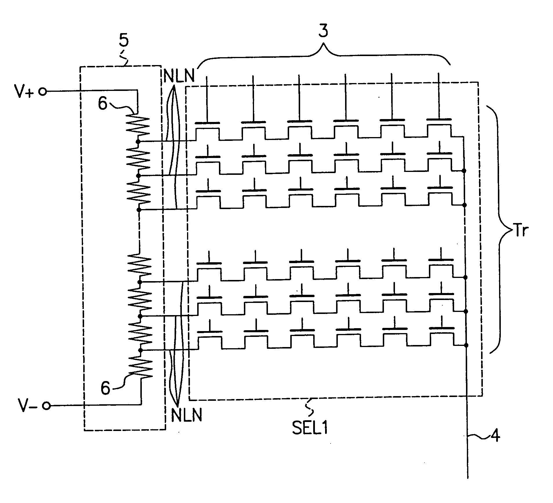
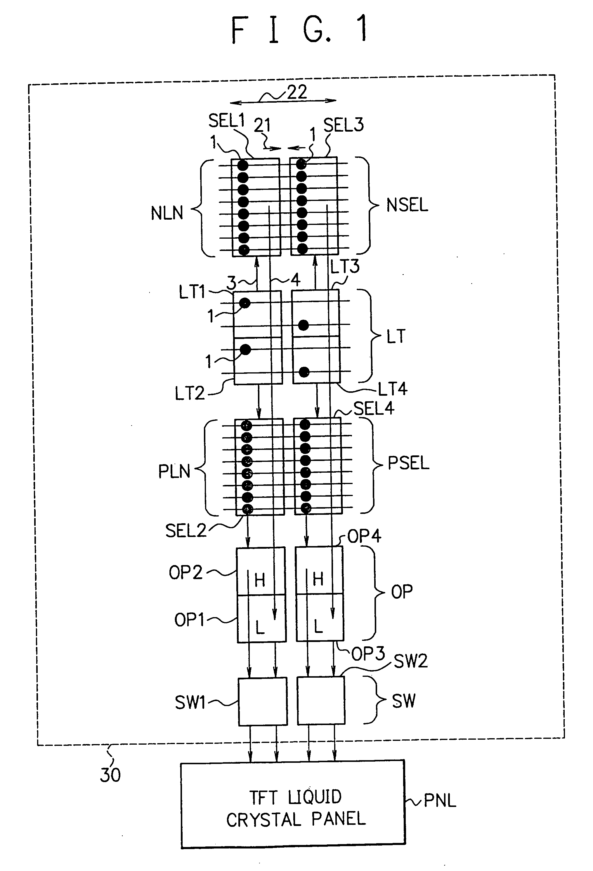
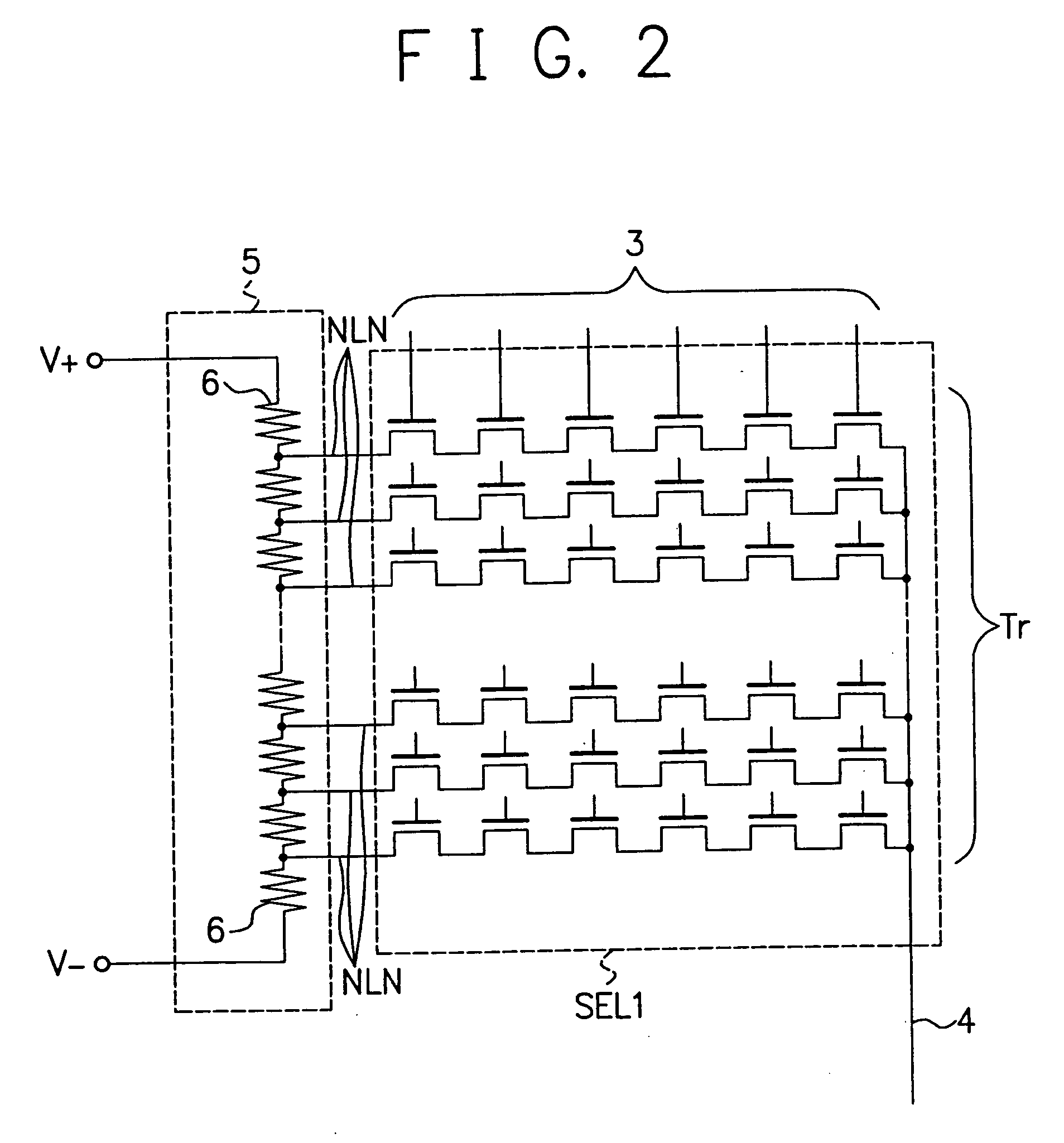
[0060]FIG. 1 is an illustration showing a construction of the first embodiment of a liquid crystal display apparatus according to the present invention. The liquid crystal display apparatus has as TFT liquid crystal panel PNL and a semiconductor integrated circuit 30 for driving the liquid crystal panel PNL. The semiconductor integrated circuit 30 includes a negative selector Portion (N-channel selector position) NSEL, a data latch portion LT, a positive selector portion (P-channel selector portion) PSEL, an operational amplifier portion OP and an output switching portion SW. In the shown embodiment of FIG. 1, the selector portion SEL in FIG. 21 is divided into the negative selector portion NSEL and the positive selector portion PSEL. On the other hand, TFT liquid crystal panel PNL is the same as that in FIG. 21.

[0061] In the data latch portion LT, a data latching line arranged immediately thereabove is connected via a wiring contact portion 1 (shown by black...

second embodiment

[0074] Second Embodiment

[0075]FIG. 3 is an illustration showing a construction of the second embodiment of the liquid crystal display apparatus according to the present invention. The liquid crystal display apparatus has the TFT liquid crystal panel PNL and the semiconductor integrated circuit 30 for driving the liquid crystal pane; In the shown embodiment, in comparison with the first embodiment (FIG. 1), vertical relationship between the negative selector portion NSEL and the upper level of the data latch portion LT is reversed and vertical relationship between the positive selector portion PSEL and the lower level of the data latch portion LT is reversed.

[0076] In the shown embodiment of the semiconductor integrated circuit 30, the negative data latch portion NLT, the negative selector portion NSEL, the positive selector portion PSEL and the positive data latch portion PLT, the operational amplifier portion OP and the output switching portion SW are arranged in sequentially orde...

third embodiment

[0078] Third Embodiment

[0079]FIG. 4 is an illustration showing a construction of the third embodiment of the liquid crystal display apparatus according to the present invention. The liquid crystal display apparatus has the TFT liquid crystal panel PNL and the semiconductor integrated circuit 30 for driving the liquid crystal panel PNL. In the shown embodiment, in comparison with the second embodiment (FIG. 3), the vertical position of the positive selector portion PSEL and the positive data latch portion PLT is reversed.

[0080] In the shown embodiment of the semiconductor integrated circuit 30, the negative data latch portion NLT, the negative selector portion NSEL, the position data latch portion PLT and the positive selector portion PSEL, the operational amplifier portion OP and the output switching portion SW are arranged vertical in the sequential order.

[0081] In the shown embodiment, the positive selector PSEL and the positive data latch PLT are taken as positive set, and the ...


PUM


Abstract

Lower level of data latch holding a digital image data and a positive selector arranged immediately above positive gradation voltage line, for selecting positive analog gradation voltage of positive gradation levels are take as a set, and upper level of data latch holding a digital image data and a negative selector arranged immediately above negative gradation voltage line, for selecting negative analog gradation voltage of negative gradation levels are take as a set. Two sets are arranged in alignment in vertical direction. A plurality of sets of vertically aligned sets are arranged horizontally to shorten a length in horizontal direction with respect to gradation voltage lines.

Description

CROSS-REFERENCE TO RELATED APPLICATIONS [0001] This application is a divisional application of application Ser. No. 09 / 733,075, filed Dec. 11, 2000, now allowed, which claims priority from Japanese Application Numbers 2000-105317 and 2000-105308, both filed Apr. 6, 2000.BACKGROUND OF THE INVENTION [0002] 1. Field of the Invention [0003] The present invention relates generally to a semiconductor integrated circuit for driving a liquid crystal panel. More particularly, the invention relates to a semiconductor integrated circuit for a liquid crystal panel outputting an analog gradation voltage for the liquid crystal display on the basis of a digital image data, a gradation wiring for a display, a driver for the liquid crystal display and a stress test method. [0004] 2. Description of the Related Art [0005]FIG. 21 is an illustration of the a construction of conventional liquid crystal display apparatus. The liquid crystal apparatus includes a thin film transistor (TFT) liquid crystal pa...

Claims


Application Information

Patent Timeline
Patent Type & Authority Applications(United States)
IPC IPC(8): G09G3/00G09G3/20G09G3/36G09G5/00G09G5/10
CPCG09G3/006G09G3/2011G09G3/3614G09G2310/0297G09G2300/0426G09G2310/027G09G3/3688Y10S345/904G09G3/36G02F1/133
Inventor YAMAGATA, SEIJIKOKUBUN, MASATOSHIUDO, SHINYA
Owner MONTEREY RES LLC
Why Eureka
Try Eureka