Data read circuit for use in a semiconductor memory and a method thereof

a data read and semiconductor technology, applied in semiconductor devices, digital storage, instruments, etc., can solve problems such as errors which could be detrimental to high-speed operation of semiconductor memory devices

Active Publication Date: 2005-02-10
SAMSUNG ELECTRONICS CO LTD
View PDF2 Cites 67 Cited by
  • Summary
  • Abstract
  • Description
  • Claims
  • Application Information

AI Technical Summary

Benefits of technology

[0020] Another exemplary embodiment of the present invention provides a data read method in a semiconductor memory device that has a memory cell array having a plurality of unit cells each of which is composed of one access transistor and one variable resistor, the method including precharging a sensing node to a power source level in response to a control signal of a first state; selecting a unit cell from the memory cell array in response to an address signal; clamping a level of a bit line of the...

Problems solved by technology

Thus, when the state of the unit cell is under the ‘SET’ state, namely, a low resistance state, the voltage of the sensing node VDL is preserved; however, when the state of the unit cell is under the ‘RESET’ sate, namely, a high resistance sta...

Method used


Image

  • Data read circuit for use in a semiconductor memory and a method thereof
  • Data read circuit for use in a semiconductor memory and a method thereof
  • Data read circuit for use in a semiconductor memory and a method thereof

Examples


Embodiment Construction

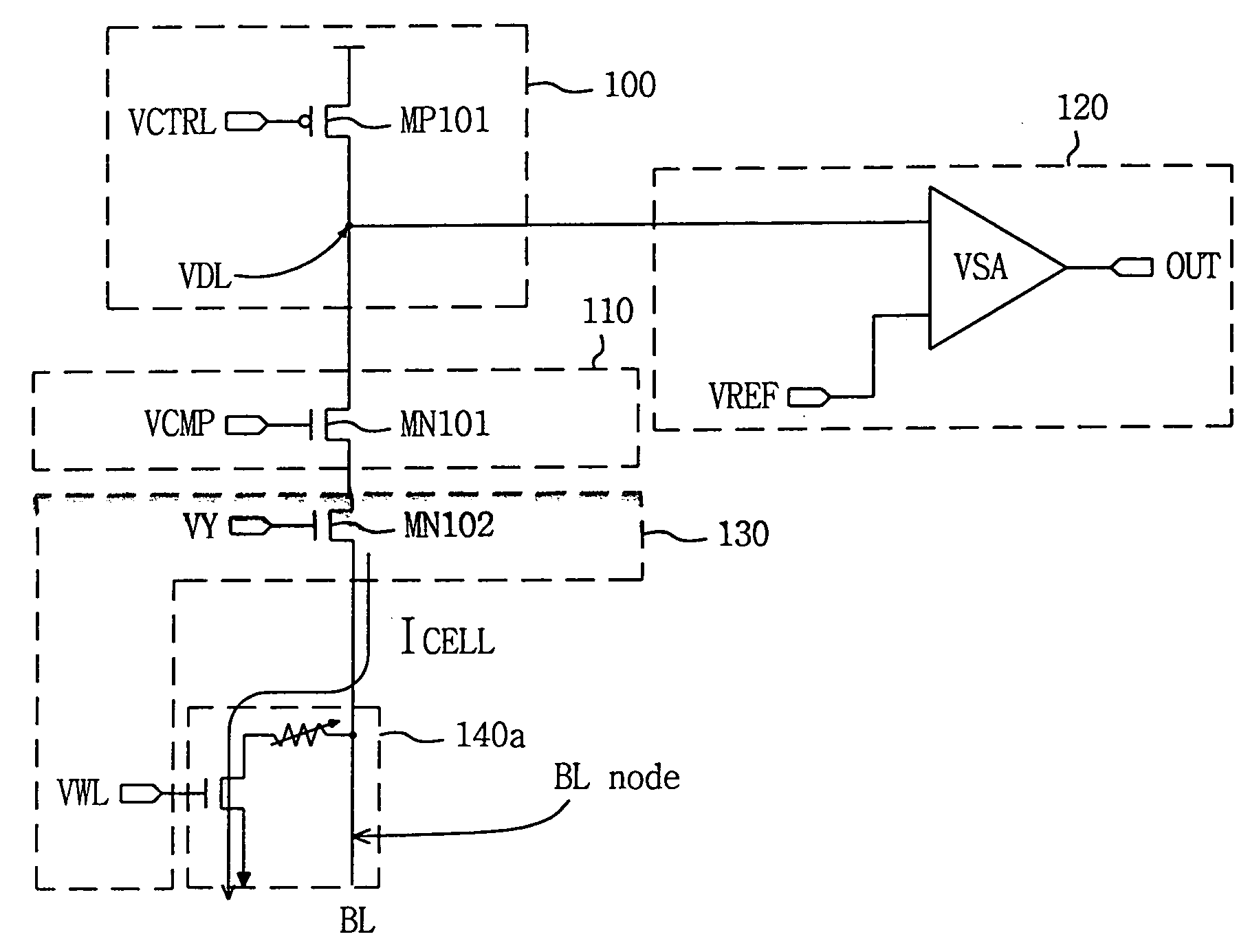
[0035] Referring to FIGS. 7 through 9, according to an exemplary embodiment of the present invention, a data read circuit includes a precharge unit 100, a clamping unit 110, a selector 130, a unit cell 140a, a memory cell array 140 (shown in FIG. 9) and a sense amplifier unit 120.

[0036] The precharge unit 100 is constructed of a positive channel metal oxide semiconductor (PMOS) control transistor MP101 in which a gate receives an applied control signal VCTRL, a source is connected to a power source, and a drain is connected to a drain of a clamping negative channel metal oxide semiconductor (NMOS) transistor MN101 of the clamping unit 110 and a sensing node VDL as an input terminal of the sense amplifier unit 120. The precharge unit 100 precharges the sensing node VDL as the power source during a precharge mode, and compensates for the sensing node VDL during a data sensing mode.

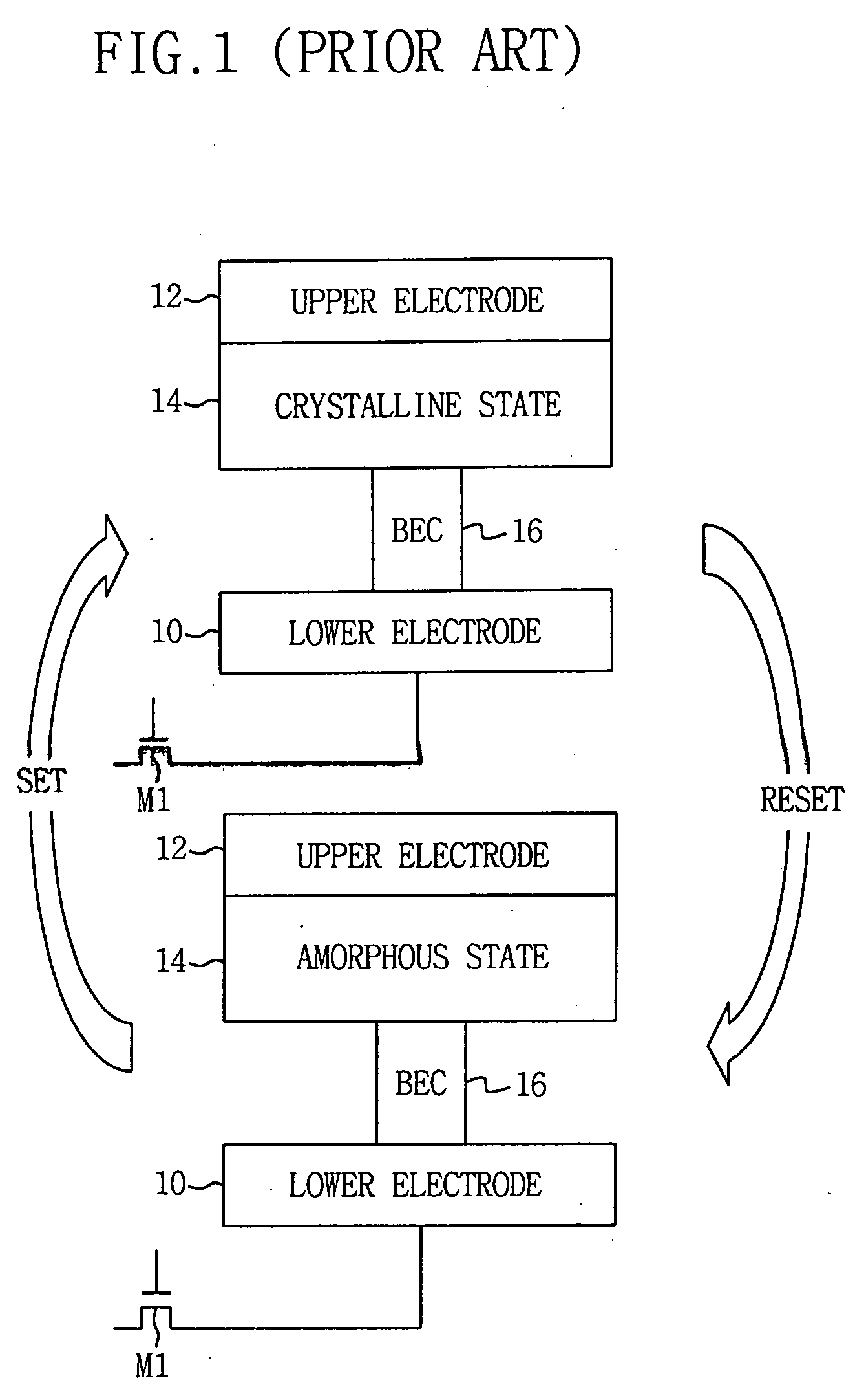
[0037] The clamping unit 110 is constructed of the clamping transistor MN101 in which a gate receives a...


PUM


Abstract

A data read circuit and method for use in a semiconductor memory device that has a memory cell array are provided. The circuit includes a selector for selecting a unit cell within the memory cell array in response to an address signal; a clamping unit for supplying a clamp voltage having a level for a read operation to a bit line of the selected unit cell in response to a clamp control signal; a precharge unit for precharging a sensing node to a voltage having a power source level in response to a control signal of a first state in a precharge mode, and compensating through the sensing node for a reduced quantity of current at the bit line in response to a control signal of a second state in a data sensing mode; and a sense amplifier unit for comparing a level of the sensing node with a reference level, and for sensing data stored in the selected unit cell.

Description

TECHNICAL FIELD [0001] The present invention relates to a semiconductor memory device, and more particularly, to a data read circuit, which includes a bias current supplier to compensate for current flowing into a unit cell and a method therefor. DISCUSSION OF THE RELATED ART [0002] The need for high performance semiconductor memories having low power consumption has led to the development of a Phase Change Random Access Memory (PRAM). The PRAM is a nonvolatile memory device for storing data by using a material such as GexSbyTez (GST) for which a phase is changed when a change in temperature changes its resistance. [0003] Referring to FIG. 1, a unit cell of a PRAM is illustrated. The unit cell of the PRAM is constructed of a transistor M1 and a variable resistor. The variable resistor includes an upper electrode 12, a phase change layer 14 that is positioned between a lower part of the upper electrode 12 and an upper part of a lower electrode contact 16, which is connected to a lowe...

Claims


Application Information

Patent Timeline
IPC IPC(8): G11C13/00G11C7/06G11C7/12G11C13/02G11C16/02G11C16/26H01L27/105H01L45/00
CPCG11C7/06G11C7/12G11C13/0004G11C2207/005G11C13/004G11C2013/0054G11C13/0026G11C13/02
Inventor OH, HYUNG-ROKCHO, WOO-YEONGKWAK, CHOONG-KEUN
Owner SAMSUNG ELECTRONICS CO LTD
Why Eureka
Try Eureka