Liquid crystal display device

a liquid crystal display and active matrix technology, applied in the direction of optics, identification means, instruments, etc., can solve the problems of deviation caused by the distribution of polarities of entire pixels, the inability to miniaturize the whole liquid crystal display device, and the difficulty in ensuring a sufficient pitch between these connection wirings, so as to reduce the scale of drive ics and prevent uneven display

Active Publication Date: 2005-02-17
JAPAN DISPLAY CENTRAL CO LTD
View PDF6 Cites 17 Cited by
  • Summary
  • Abstract
  • Description
  • Claims
  • Application Information

AI Technical Summary

Benefits of technology

[0013] It is an object of the present invention to provide a liquid crystal display device capable of reducing the scale of drive ICs and preventing uneven display in the case of adopting signal line selective drive.
[0016] Moreover, as to the Lth scan line, for each of the groups, the signal line to which the video signal having its polarity inverted between the L-1th scan line and the Lth scan line is supplied is selected first and the signal line to which the video signal having its polarity not inverted is supplied is selected later. Specifically, the video signal having the polarity not inverted has no potential change and adjacent signal lines are not influenced by the potential change. Thus, such a video signal is supplied to the signal line later. Consequently, all the signal lines can write the video signals into the pixels without being influenced by the potential change.
[0017] As described above, according to the present invention, by reducing the scale of the drive ICs, cost reduction can be achieved and power consumption can be suppressed. Moreover, since all the signal lines are not influenced by the potential change, potentials of the respective pixels are not changed. Accordingly, uneven display can be prevented. Thus, a liquid crystal display device capable of high-quality image display can be realized.

Problems solved by technology

Thus, it was impossible to miniaturize the whole liquid crystal display device.
Thus, it is difficult to secure a sufficient pitch between these connection wirings.
However, when the V line inversion drive method is applied to the signal line selective drive, there is a deviation caused in a distribution of polarities for entire pixels.
Thus, there is a problem that display failure called a crosstalk, which has a tail along a window pattern in displaying the window pattern, is likely to occur.
Moreover, when the H / V inversion drive method is applied to the signal line selective drive, since an inversion cycle of video signals is short, in addition to a conventional problem such as increased power consumption, there is the following problem.
Thus, there is a problem that there occurs a difference in write potentials into pixels for each signal line and uneven display occurs.

Method used


Image

  • Liquid crystal display device
  • Liquid crystal display device
  • Liquid crystal display device

Examples


first embodiment

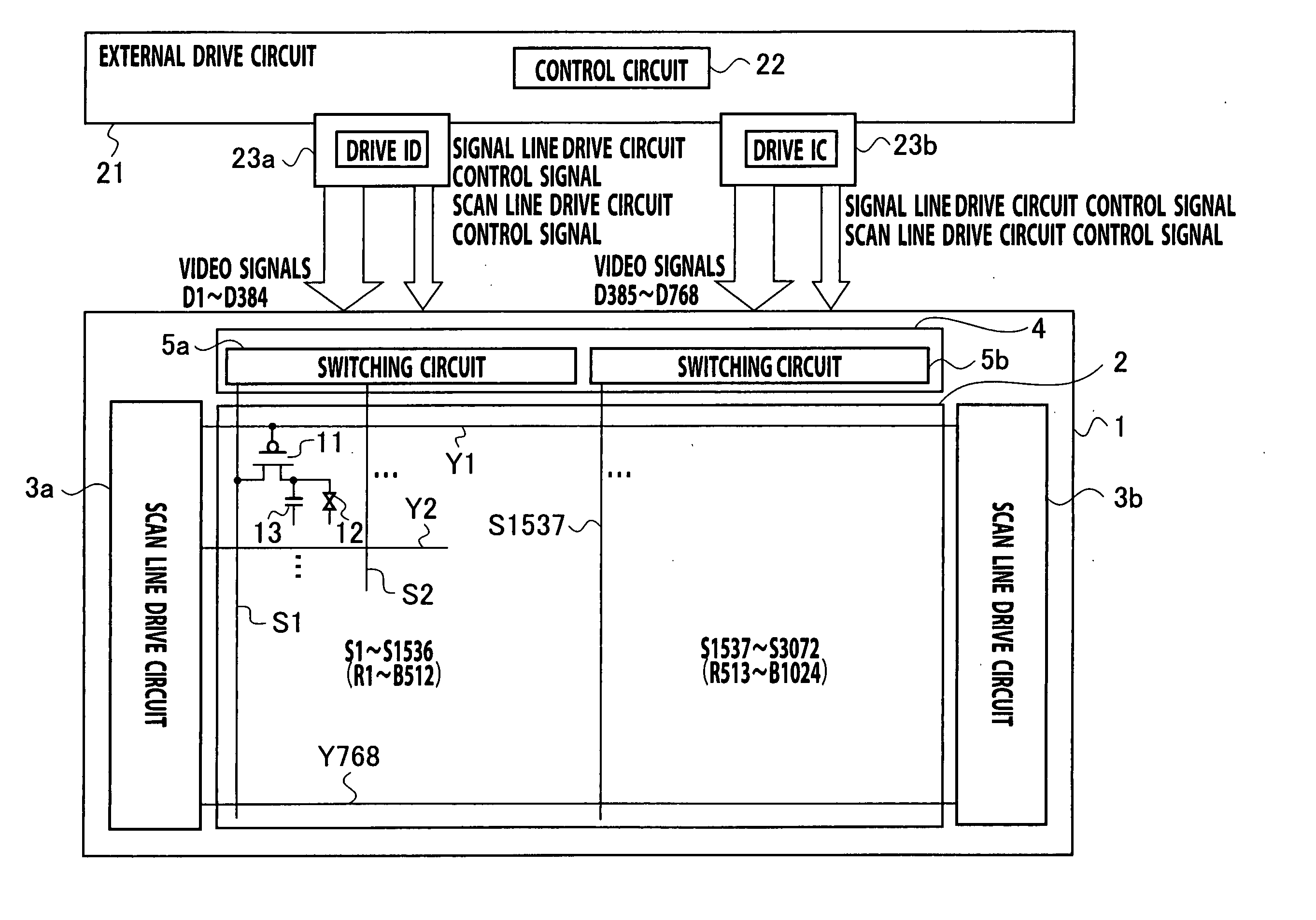
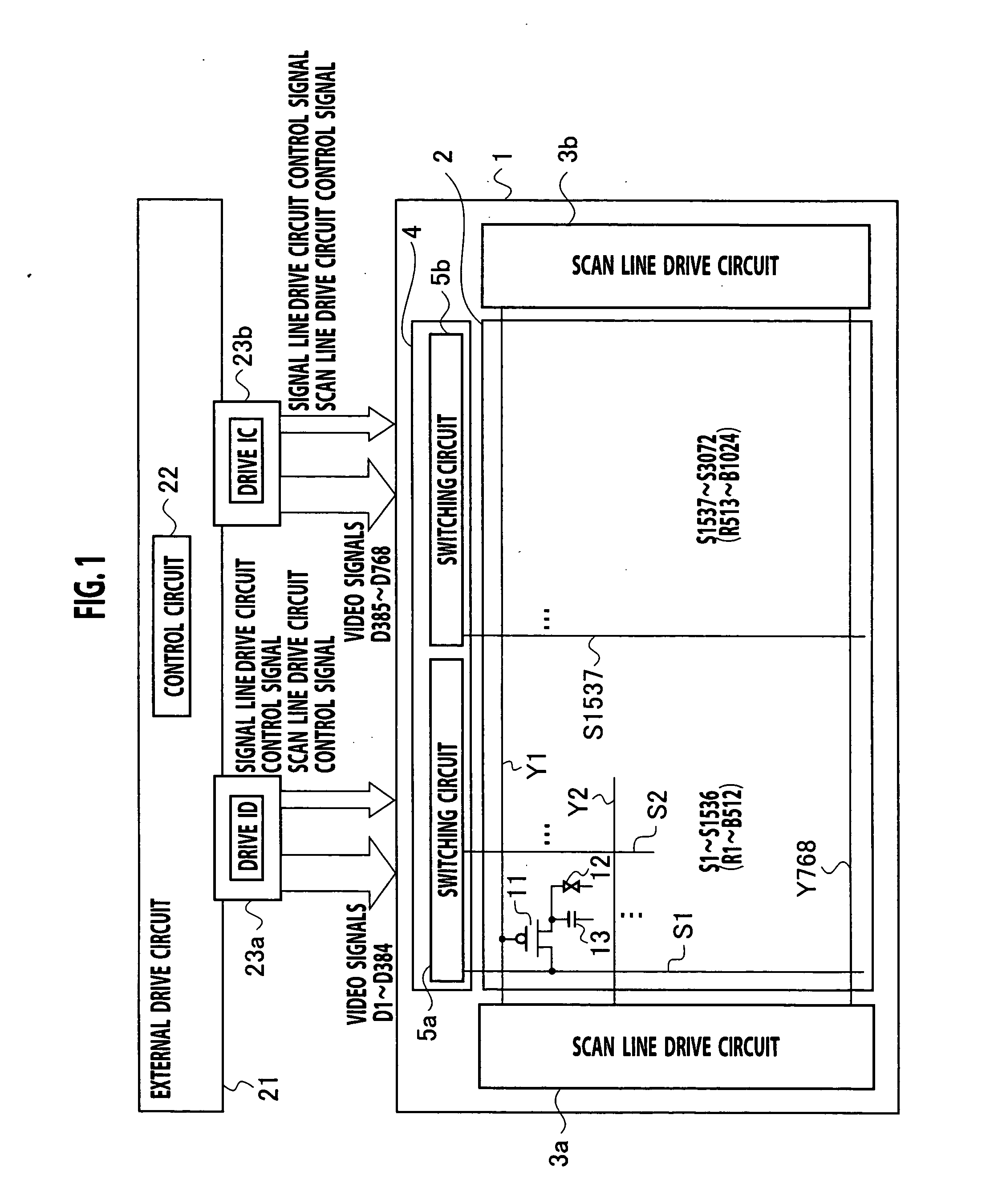
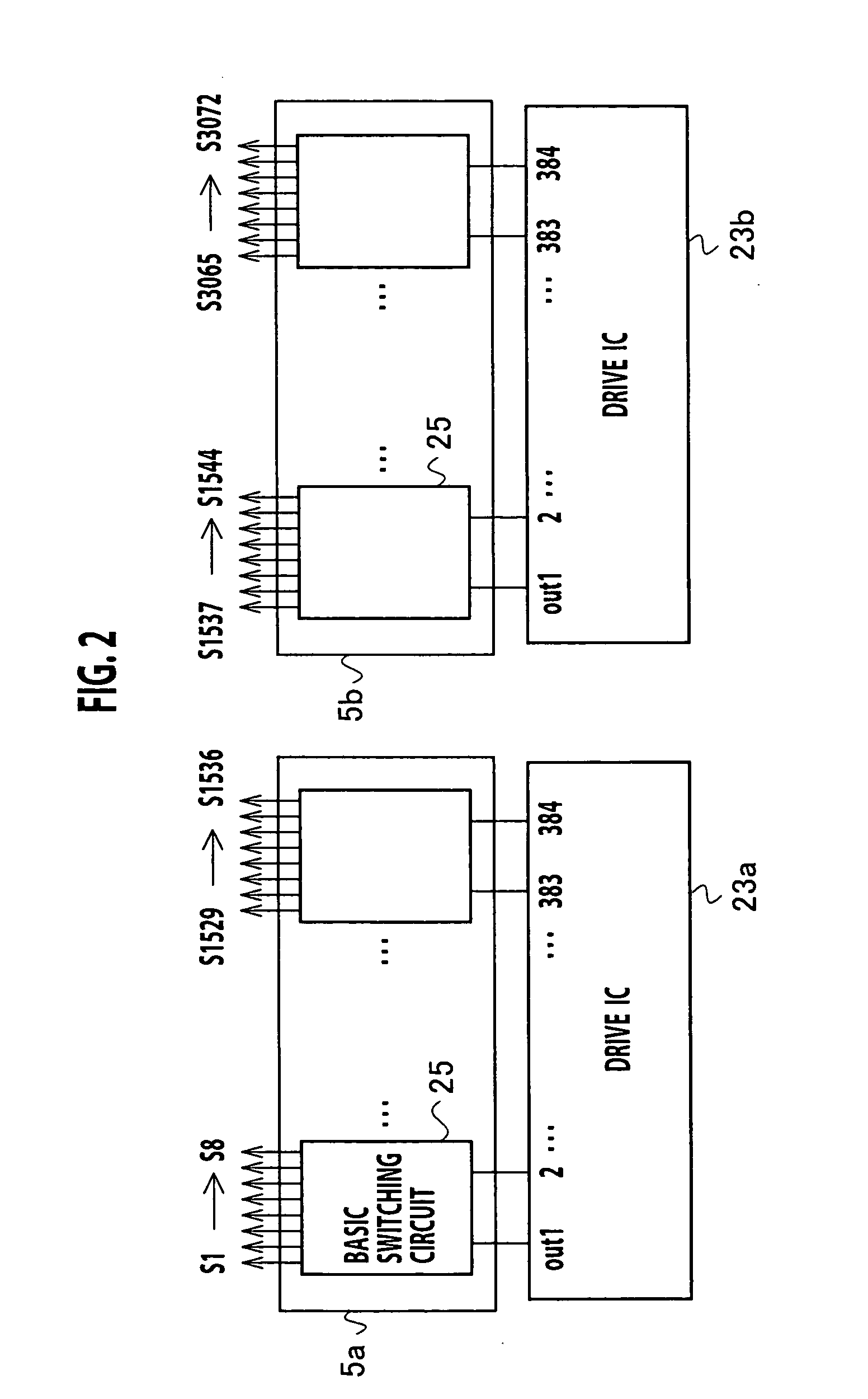
[0062] As shown in a circuit block diagram of FIG. 1, a liquid crystal display device of this embodiment includes, a pixel display part 2 on a glass array substrate 1; scan line drive circuits 3a and 3b which are disposed at both left and right ends of the pixel display part 2; and a signal line drive circuit 4 which is disposed at an upper end of the pixel display part 2. In addition, the liquid crystal display device includes an external drive circuit 21 and drive ICs 23a and 23b outside the array substrate 1.

[0063] In the pixel display part 2, a plurality of scan lines Y1 to Y768 from the scan line drive circuits 3 and a plurality of signal lines S1 to S3072 from the signal line drive circuit 4 are arranged so as to intersect with each other. At respective intersections, pixels, each including a thin film transistor 11, a liquid crystal capacity 12 and an auxiliary capacity 13, are disposed. The thin film transistor 11 is, for example, a MOS-TFT, which has its drain terminal con...

second embodiment

[0098] As described in the first embodiment, in the case of supplying a video signal by switching the video signal to a plurality of signal lines in one horizontal scan period, the larger the number of signal lines is, the shorter the time for supplying the video signal to each of the signal lines (hereinafter referred to as write time) becomes. Thus, selection of the signal lines is terminated before write of a desired analog potential into pixels through the signal lines is finished. Accordingly, write deficiency into pixels may occur.

[0099] There are two factors causing the write deficiency, including: (i) polarity inversion of a video signal between the L-1th line and the Lth line (hereinafter referred to as “polarity inversion in a vertical direction”); and (ii) polarity inversion of a video signal between a signal line selected to be an S-1th (S is an integer of 1 or more) and a signal line selected to be an Sth (hereinafter referred to as “polarity inversion in a horizontal ...

third embodiment

[0112] As shown in an equivalent circuit of FIG. 11, each pixel is connected to its own signal line S1 via a coupling capacity Cp1 and is connected to an adjacent signal line S2 via a coupling capacity Cp2. Moreover, each pixel is connected to pixels positioned thereabove and therebelow via coupling capacities Cp3. In FIG. 11, Clc is a liquid crystal capacity and Ccs is an auxiliary capacity.

[0113] A potential change amount which each pixel electrode receives via the coupling capacity Cp1 due to a potential change dVsig_m (sig_m is the number of a signal line) of the own signal line S1 is assumed to be Vs. A potential change amount which each pixel electrode receives via the coupling capacity Cp2 due to a potential change dVsig_m+1 of the adjacent signal line S2 is assumed to be Vn. A potential change amount which each pixel electrode receives via the coupling capacity Cp3 due to a potential change dVpix of a lower pixel is assumed to be Vv. At this time, Vs, Vn and Vv can be expre...


PUM

PropertyMeasurementUnit
polarityaaaaaaaaaa
color reproductionaaaaaaaaaa
polaritiesaaaaaaaaaa

Abstract

In order to reduce the scale of drive ICs and to prevent uneven display in signal line selective drive, in this liquid crystal display device, for each group in which one video output line corresponds to N signal lines, the signal line is switched and connected to the video output line via an analog switch ASW. Thus, the number of the video output lines is reduced to 1 / N. Moreover, as to an Lth scan line, for each of the groups, a signal line to which a video signal having its polarity inverted between an L-1th scan line and the Lth scan line is supplied is selected first and a signal line to which a video signal having its polarity not inverted is supplied is selected later. Thus, a video signal in which a polarity is not inverted and no potential change occurs is supplied to the signal line later.

Description

CROSS-REFERENCE TO RELATED APPLICATIONS [0001] This application is based upon and claims the benefit of priority from Japanese Patent Application No. 2003-293318 filed Aug. 14, 2003 and Japanese Patent Application No. 2004-40128 filed Feb. 17, 2004; the entire contents of which are incorporated herein by reference. BACKGROUND OF THE INVENTION [0002] 1. Field of the Invention [0003] The present invention relates to an active matrix liquid crystal display device. [0004] 2. Description of the Related Art [0005] In a word processor, a personal computer, a portable TV and the like, a thin and lightweight display device is widely used. Particularly, since it is easy to realize a thin and lightweight liquid crystal display device with low power consumption, there has been extensive development of the liquid crystal display device. Accordingly, a liquid crystal display device with high resolution and a large-sized screen has been available at a relatively low price. [0006] Among the liquid ...

Claims


Application Information

Patent Timeline
Patent Type & Authority Applications(United States)
IPC IPC(8): G09F9/30G02F1/133G09G3/20G09G3/36
CPCG09G3/3614G09G3/3648G09G2320/0233G09G2310/0297G09G2320/0209G09G3/3688G02F1/133G09G3/36
Inventor KITANI, MASAKATSUMIYATAKE, MASAKI
Owner JAPAN DISPLAY CENTRAL CO LTD
Why Eureka
Try Eureka