Singulation method used in leadless packaging process

a leadless packaging and process technology, applied in semiconductor devices, semiconductor/solid-state device details, electrical equipment, etc., can solve the problems of reducing the service life of the blad

Inactive Publication Date: 2005-02-17
ADVANCED SEMICON ENG INC
View PDF4 Cites 17 Cited by
  • Summary
  • Abstract
  • Description
  • Claims
  • Application Information

AI Technical Summary

Benefits of technology

[0011] It is therefore an object of the present invention to provide a singulation method used in a leadl

Problems solved by technology

However, as integrated circuits products move its endless pace toward both a faster speed and a smaller size, the traditional lead frame packages have become gradually obsolete for some high performance-required packages.
Traditional lead frame package has its limit of providing a solution for chip scale and low profile package due to the long inner leads and outer leads.
One major problem during the manufact

Method used


Image

  • Singulation method used in leadless packaging process
  • Singulation method used in leadless packaging process
  • Singulation method used in leadless packaging process

Examples


Embodiment Construction

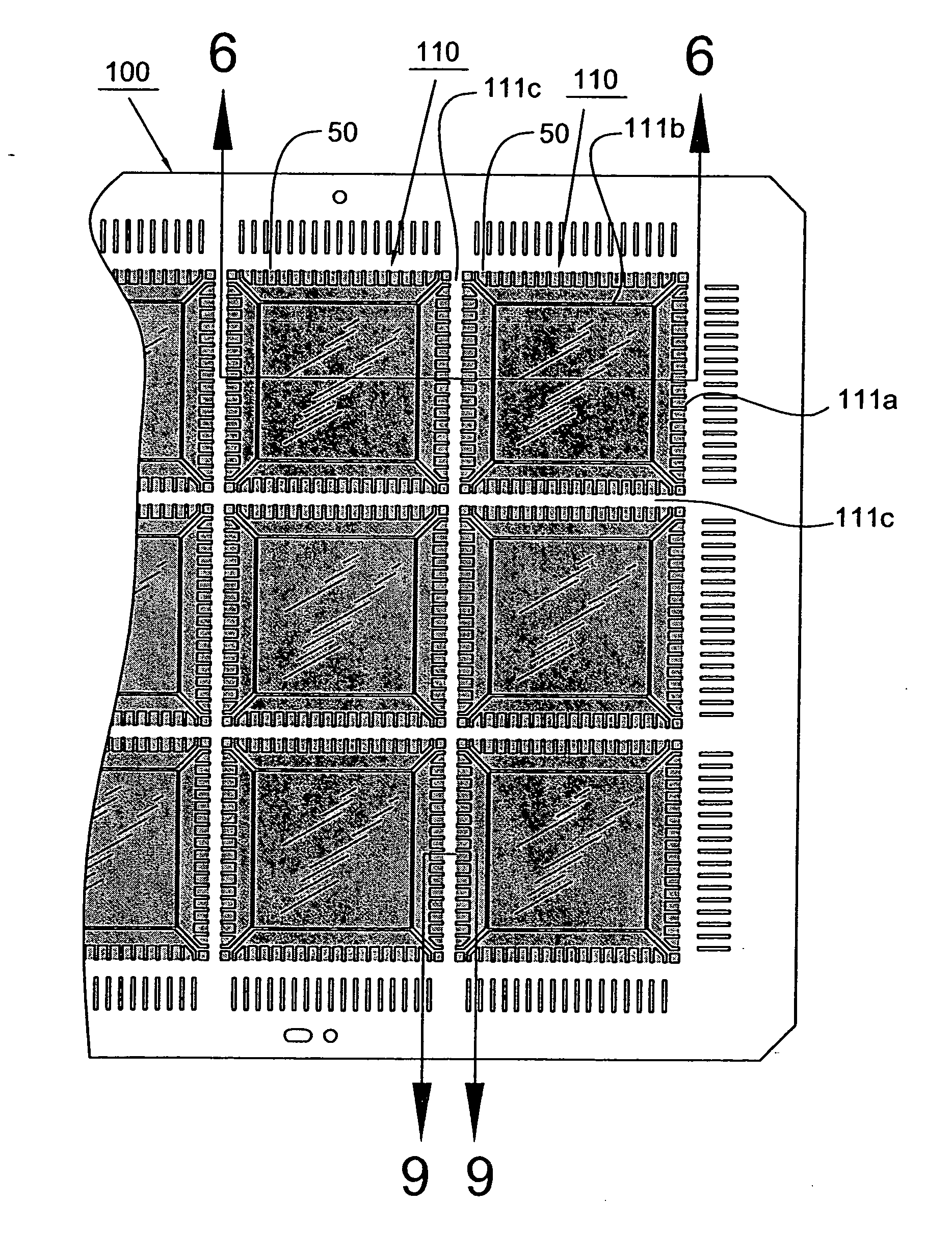
[0028]FIG. 4 shows an array of molded products 50 which are hatched in FIG. 4 to facilitate understanding. The molded products 50 are provided on a lead frame 100. The lead frame 100 has an upper surface and a lower surface opposed to the upper surface. The lead frame 100 comprises a plurality of units 110 each including a plurality of leads 111a arranged at the periphery of a die pad 111b. The units 110 of the lead frame 100 are separated from each other by a plurality of dambars 111c. The dambars 111c generally form an orthogonal grid on the lead frame 100. Specifically, the dambars 111c are defined between the leads 111a at the periphery of the die pads 111b. The lead frame 100 is typically made of a copper-base alloy or made of copper or alloys containing copper, and shaped by pressing or etching. Lead frames suitable for use in the present invention are available in three lead finishes: post plated SnPb and Matte Sn, and pre plated Ni / Pd with flash of Au (i.e., PPF (Pre-Plating...


PUM


Abstract

A singulation method used in leadless packaging process is disclosed. An array of molded products on an upper surface of a lead frame is utilized in the singulation method. The lead frame has a plurality of dambars between the molded products. The lower surface of the lead frame is attached with a tape. Each of the molded products includes a semiconductor chip encapsulated in a package body and electrically coupled to the upper surface of the lead frame. The singulation method is accomplished by etching the upper surface of the lead frame with the package bodies as mask until each dambar is etched away.

Description

BACKGROUND OF THE INVENTION [0001] 1. Field of the Invention [0002] This invention relates to a process for making leadless semiconductor packages and more specifically to a singulation method used in the leadless packaging process. [0003] 2. Description of the Related Art [0004] Lead frame packages have been used for a long period of time in the IC packaging history mainly because of their low manufacturing cost and high reliability. However, as integrated circuits products move its endless pace toward both a faster speed and a smaller size, the traditional lead frame packages have become gradually obsolete for some high performance-required packages. Thus BGA (Ball Grid Array Packages) and CSP (Chip Scale Package) have emerged and become increasingly popular as a new packaging choice. The former has been widely used in IC chips that have higher I / Os and need better electrical and thermal performance than the conventional packages such as CPU and graphic chips. The latter has been ...

Claims


Application Information

Patent Timeline
IPC IPC(8): H01L21/48H01L21/56H01L21/68H01L23/31
CPCH01L21/4828H01L2924/01005H01L21/566H01L21/568H01L23/3107H01L24/97H01L2224/32245H01L2224/48091H01L2224/48247H01L2224/73265H01L2224/97H01L2924/01029H01L2924/01046H01L2924/01047H01L2924/01078H01L2924/01079H01L2924/01082H01L2924/3011H01L21/561H01L24/48H01L2924/10253H01L2924/01076H01L2924/01033H01L2924/01006H01L2924/00014H01L2224/85H01L2924/00012H01L2924/00H01L2924/181H01L24/73H01L2224/05599H01L2224/45099H01L2224/85399H01L2924/14H01L2224/45015H01L2924/207
Inventor LEE, JUN HONGPARK, HYUNG JUNKIM, HYEONG NOKANG, KUN A.
Owner ADVANCED SEMICON ENG INC
Why Eureka
Try Eureka