Photo-electric converting device and its driving method, and its manufacturing method, solid-state image pickup device and its driving method and its manufacturing method

a technology of photoelectric converting and driving method, which is applied in the direction of radio frequency controlled devices, television system scanning details, etc., can solve the problems of 53/b>, the light incident on the photo-electric converting portion cannot obtain sufficient sensitivity, etc., and achieves suppression of an increase of dark current and high sensitivity characteristics.

Active Publication Date: 2005-02-24
SONY SEMICON SOLUTIONS CORP
View PDF3 Cites 88 Cited by
  • Summary
  • Abstract
  • Description
  • Claims
  • Application Information

AI Technical Summary

Benefits of technology

[0030] In view of the aforesaid aspect, it is an object of the present invention to provide a photo-electric converting device, its driving method and its manufacturing method in which a high sensitivity characteristic and suppression of an increase of a dark current caused by interface states can be achieved at the same time.

Problems solved by technology

As a consequence, an amount of light that becomes incident on the photo-electric converting portion 53 decreases finally, and a problem arises, in which the photo-electric converting portion 53 cannot obtain sufficient sensitivity.

Method used


Image

  • Photo-electric converting device and its driving method, and its manufacturing method, solid-state image pickup device and its driving method and its manufacturing method
  • Photo-electric converting device and its driving method, and its manufacturing method, solid-state image pickup device and its driving method and its manufacturing method
  • Photo-electric converting device and its driving method, and its manufacturing method, solid-state image pickup device and its driving method and its manufacturing method

Examples


Embodiment Construction

[0059] The present invention will be described below with reference to the drawings.

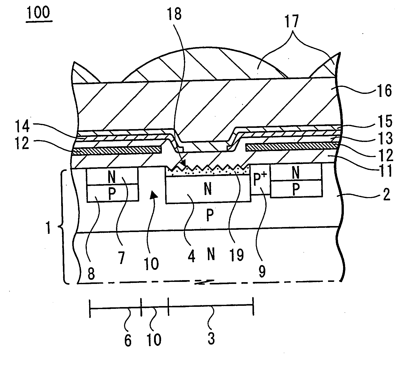
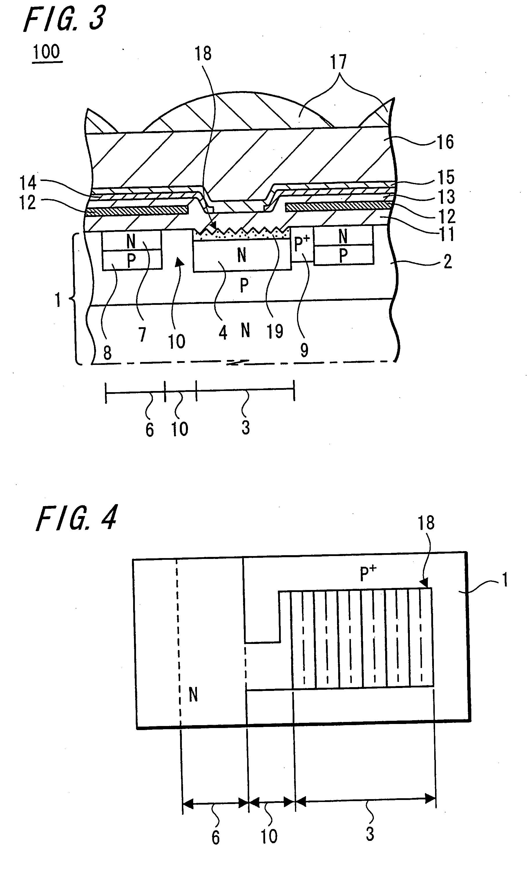
[0060] First, a solid-state image pickup device according to an embodiment of the present invention will be described with reference to FIG. 3 which is an enlarged cross-sectional view.

[0061] As shown in FIG. 3, a solid-state image pickup device 100 according to this embodiment includes an N-type silicon semiconductor substrate 1 which is mainly made of high-purity single crystal silicon (Si) in which a P-type first semiconductor well layer 2 is formed. A photo-diode formed of an N-type semiconductor region (so-called electric charge accumulating region) 4, for example, comprising a photo-electric converting portion 3 is formed on the surface side of the semiconductor substrate 1.

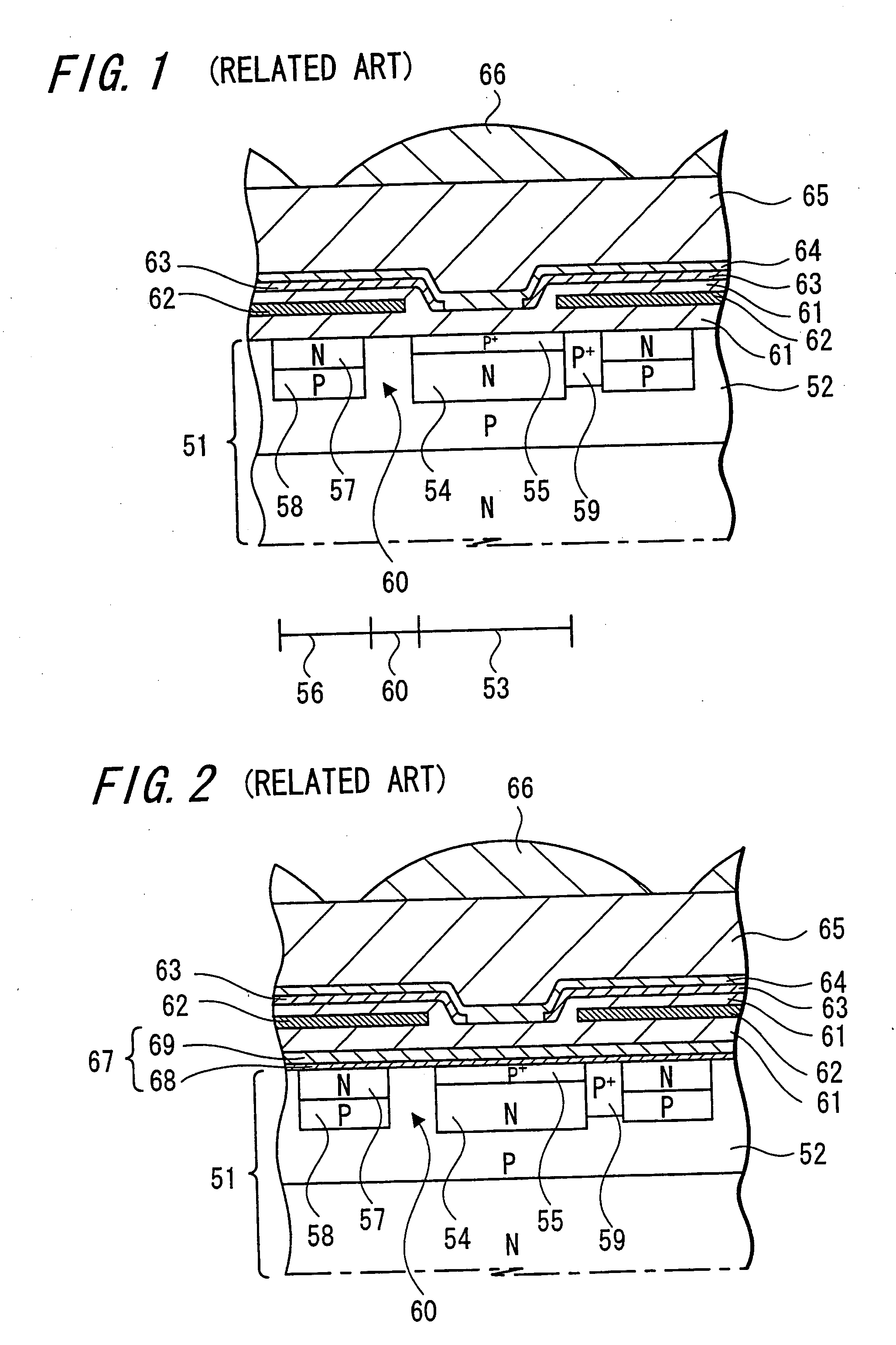
[0062] An N-type transfer channel region 7 comprising a vertical CCD portion 6 is formed on one side of the row of the photo-electric converting portion 3, and a P-type second semiconductor well region 8 is formed under t...


PUM


Abstract

A photo-electric converting apparatus 100 has an arrangement in which a photo-electric converting apparatus 3 is formed on the surface of a substrate 1, an insulating film 11 is formed on the substrate 1, an uneven portion 18 having concavities and convexities in the thickness direction of the substrate 1 is formed on at least a part of the interface between the substrate 1 of the photo-electric converting portion 3 and the insulating film 11 and a recombination region 19 for decreasing a dark current is formed so as to contain the uneven portion 18 within the photo-electric converting portion 3. This photo-electric converting apparatus becomes able to obtain a high sensitivity characteristic and to suppress a dark current from being increased by a decrease of the interface states.

Description

BACKGROUND OF THE INVENTION [0001] 1. Field of the Invention [0002] The present invention relates to a photo-electric converting device and its driving method, and its manufacturing method. Also, the present invention relates to a solid-state image pickup device, and its driving method and its manufacturing method. [0003] 2. Description of the Related Art [0004] A solid-state image pickup device, for example, an ordinary solid-state image pickup device includes a plurality of photo-electric converting portions like photo-diodes arrayed as light-receiving cells in a one-dimensional fashion (linearly) or in a two-dimensional fashion (in a matrix fashion) on the surface of a semiconductor substrate. When light becomes incident on each of those photo-electric converting portions, signal charges are generated in response to the light and those signal charges are read out by a transfer electrode as a video signal. [0005]FIG. 1 of the accompanying drawings is a cross-sectional view showing...

Claims


Application Information

Patent Timeline
Patent Type & Authority Applications(United States)
IPC IPC(8): H01L21/76H01L27/14H01L27/146H01L27/148H01L29/74H01L29/768H01L31/0352H01L31/10H04N5/335H04N5/359H04N5/361H04N5/369H04N5/3725
CPCH01L27/1462H01L27/14627H01L27/14687H01L31/0352H01L27/14806H01L27/14812H01L27/1485H01L27/14689H01L27/146H01L31/10
Inventor MURAKAMI, ICHIRO
Owner SONY SEMICON SOLUTIONS CORP
Why Eureka
Try Eureka