Area array type package stack and manufacturing method thereof

a technology of area array and package stack, which is applied in the direction of electrical apparatus, semiconductor/solid-state device details, semiconductor devices, etc., can solve the problems of increasing package size, increasing mounting density, and reducing yield losses, so as to reduce the height of the package stack

Inactive Publication Date: 2005-02-24
SAMSUNG ELECTRONICS CO LTD
View PDF9 Cites 106 Cited by
  • Summary
  • Abstract
  • Description
  • Claims
  • Application Information

AI Technical Summary

Benefits of technology

[0009] At least one embodiment of the present invention provides a stack of area array type packages, such as ball grid array (BGA) packag...

Problems solved by technology

However, chip stack package 100 encounters potential reliability test failures and resultant yi...

Method used


Image

  • Area array type package stack and manufacturing method thereof
  • Area array type package stack and manufacturing method thereof
  • Area array type package stack and manufacturing method thereof

Examples


Embodiment Construction

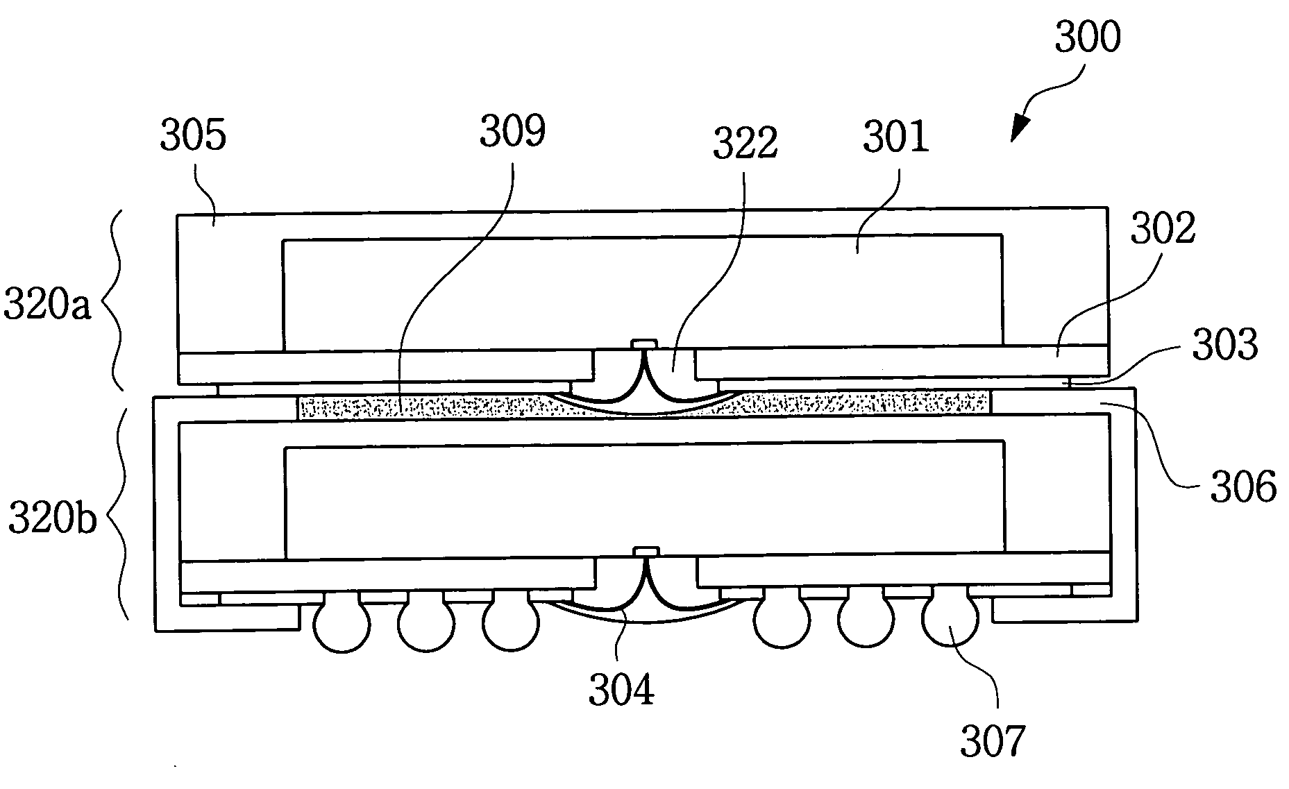
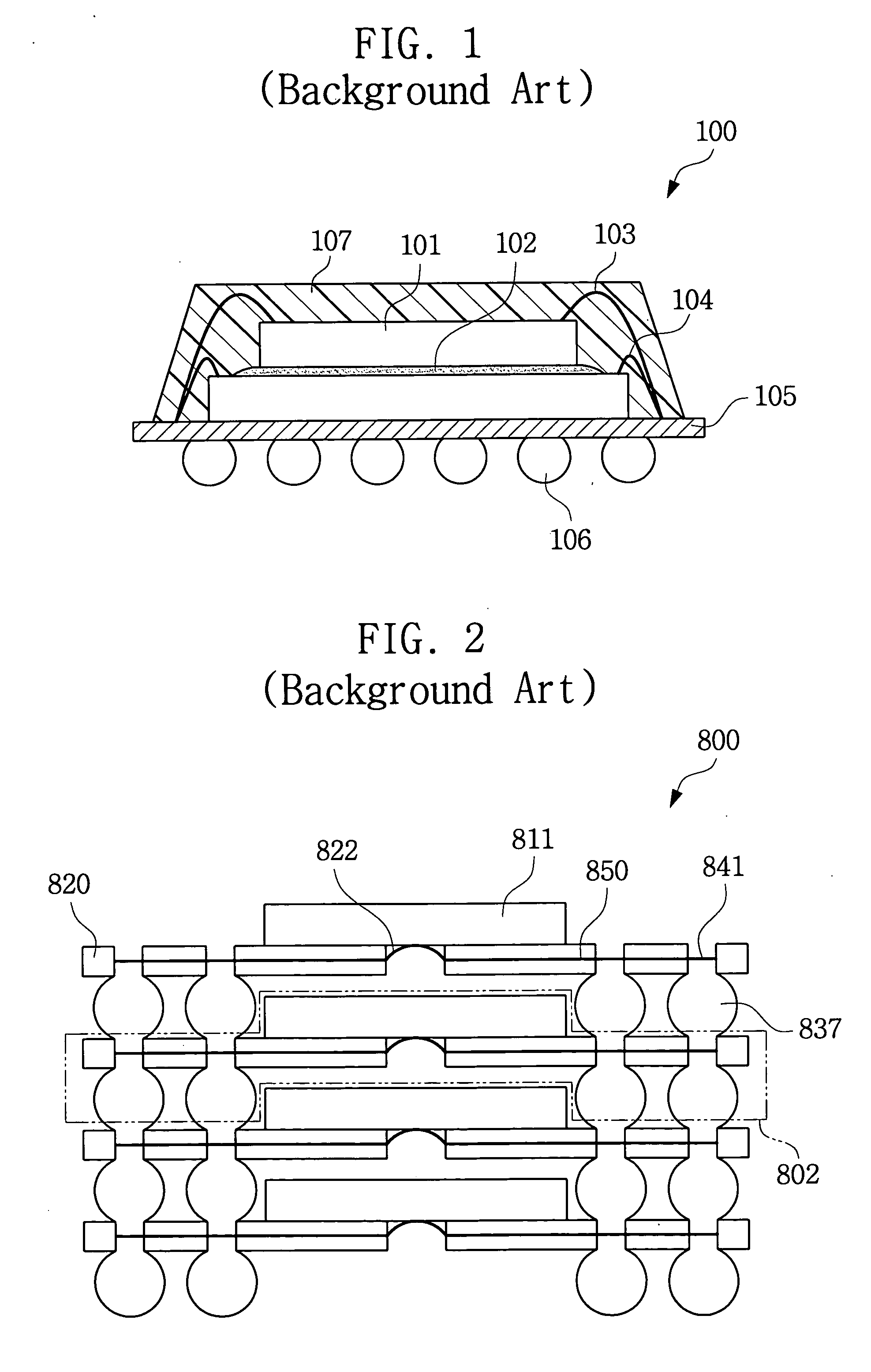
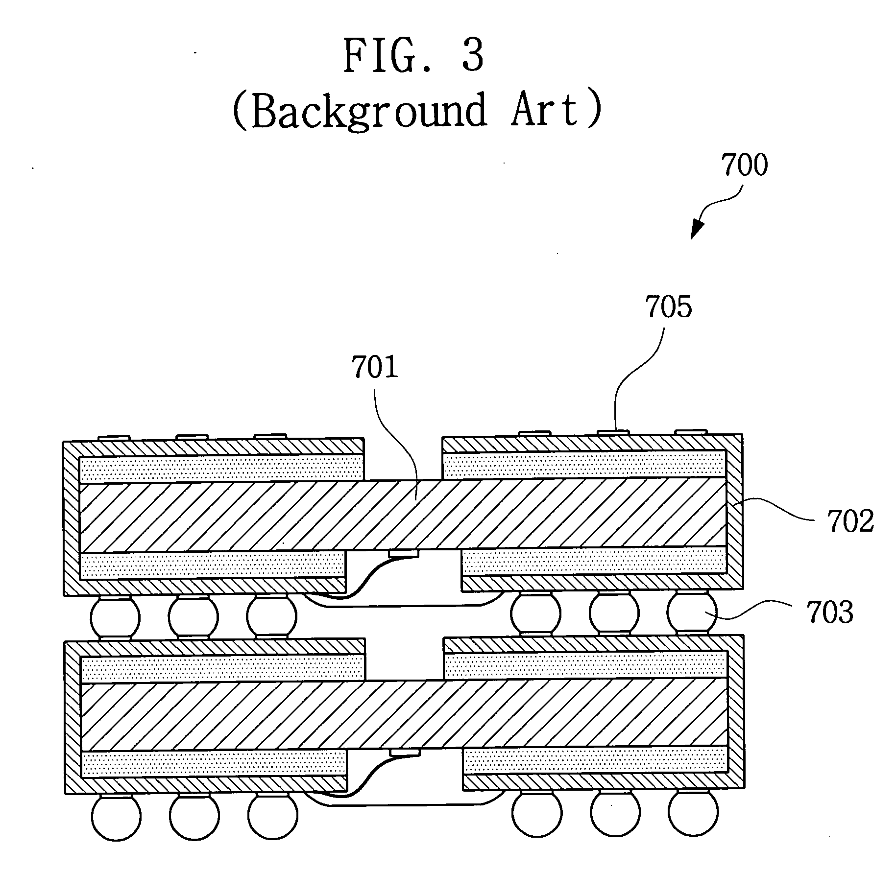
[0027] The present invention will now be described more fully hereinafter with reference to the accompanying drawings, in which example embodiments of the present invention are shown. The present invention may, however, be embodied in many different forms and should not be construed as limited to the embodiments set forth herein. Rather, these embodiments are provided so that this disclosure will be thorough and complete, and will fully convey the scope of the invention to those skilled in the art.

[0028] In the description, well-known structures and processes have not been shown in detail for the sake of brevity and to avoid obscuring the present invention. It will be appreciated that for simplicity and clarity of illustration, some elements illustrated in the figures have not necessarily been drawn to scale. For example, the dimensions of some of the elements are exaggerated relative to other elements for clarity. Like numerals are used for like and corresponding parts of the vari...


PUM


Abstract

A package stack has at least two packages of area array types (AAT), each having connecting pads. A flexible cable having conductive patterns is provided between the AAT packages and electrically connected to the connecting pads of the packages.

Description

CROSS REFERENCE TO RELATED APPLICATIONS [0001] This U.S. non-provisional application claims priority under 35 U.S.C. §119 to Korean Patent Application No. 2003-58273 filed Aug. 22, 2003, the contents of which are incorporated by reference.BACKGROUND OF THE PRESENT INVENTION [0002] A kind of packaging technology generally known in the Background Art is a three-dimensional stacking. Such stacking technology, including chip stacking and package stacking, serves to increase the number of chips or packages per unit area of the motherboard (or, in other words, to increase density). [0003] A typical chip stack package 100, also referred to as a multi-chip package (MCP), is shown in FIG. 1, according to the Background Art. Referring to FIG. 1, chip stack package 100 has two chips 101 and 102 stacked on a common substrate 105. Respective chips 101 and 102 are electrically connected to substrate 105 through bond wires 103 and 104. An encapsulating body 107 protects chips 101 and 102 and wires...

Claims


Application Information

Patent Timeline
IPC IPC(8): H01L23/31H01L23/498H01L23/12H01L25/10
CPCH01L23/3128H01L2224/06136H01L23/49833H01L23/4985H01L25/105H01L2224/32145H01L2224/48091H01L2224/48227H01L2224/4824H01L2924/14H01L2924/15311H01L2924/15331H01L23/49811H01L2224/06135H01L2924/07802H01L2224/73215H01L2224/32225H01L2224/73265H01L2225/1041H01L2225/1023H01L24/48H01L2924/00014H01L2924/00012H01L2924/00H01L24/73H01L2224/45099H01L2224/45015H01L2924/207H01L23/12
Inventor LEE, JONG-JOO
Owner SAMSUNG ELECTRONICS CO LTD
Why Eureka
Try Eureka