Package structure

A technology of packaging structure and core structure, applied in the direction of semiconductor/solid-state device components, semiconductor devices, electrical components, etc., can solve the problems affecting the heat dissipation performance of electronic devices or packaging structures, poor heat dissipation, etc., to reduce the height of the package and improve the The effect of cooling efficiency

Active Publication Date: 2021-02-19
UNIMICRON TECH CORP
View PDF9 Cites 0 Cited by
  • Summary
  • Abstract
  • Description
  • Claims
  • Application Information

AI Technical Summary

Problems solved by technology

However, embedded components often face the problem of poor heat dissipation, which in turn affects the overall heat dissipation performance of electronic devices or packaging structures

Method used


Image

  • Package structure
  • Package structure
  • Package structure

Examples


Embodiment Construction

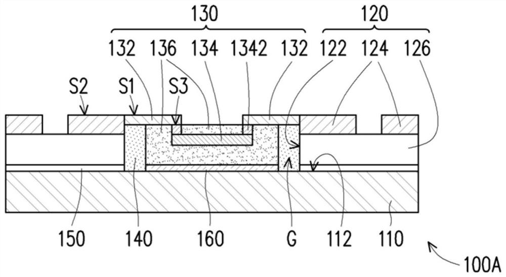
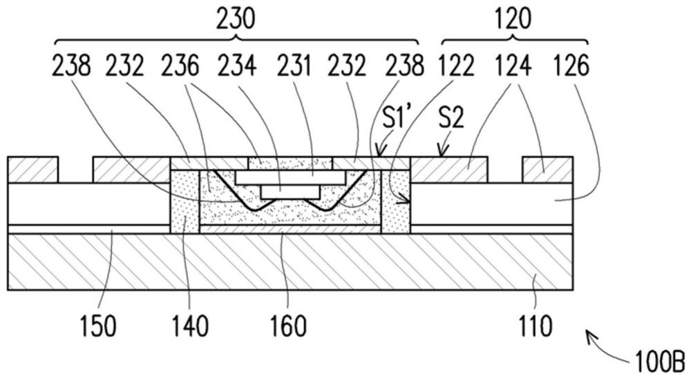
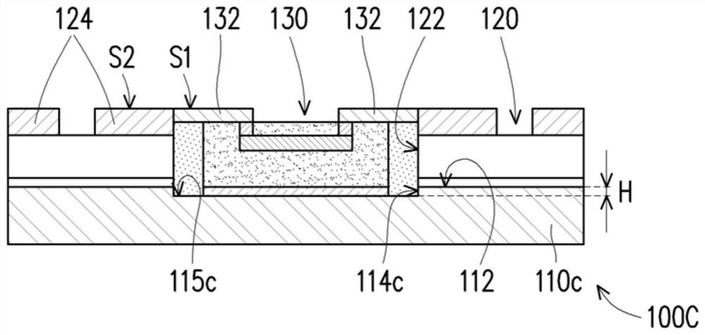
[0060] figure 1 A schematic cross-sectional view showing a package structure according to an embodiment of the present invention. Please refer to figure 1 , the package structure 100A of this embodiment includes a metal substrate 110 , a core structure layer 120 and a package component 130 . The core structure layer 120 is disposed on the metal substrate 110 and has an opening 122 and a patterned conductive layer 124 . The packaging component 130 is disposed on the metal substrate 110 and located in the opening 122 of the core structure layer 110 . The package component 130 includes a plurality of external leads 132 , and each external lead 132 is electrically connected to the patterned conductive layer 124 of the core structure layer 120 . In particular, the outer surface S1 of each outer lead 132 is aligned with the upper surface S2 of the patterned conductive layer 124 .

[0061] In detail, the metal substrate 110 of this embodiment has a disposition surface 112 , and t...


PUM


Abstract

The invention provides a packaging structure, which includes a metal substrate, a core structure layer and packaging components. The core structure layer is configured on the metal substrate, and has an opening and a patterned conductive layer. The packaging element is disposed on the metal substrate and located in the opening of the core structure layer. The packaging component includes a plurality of external leads, and the external leads are electrically connected to the patterned conductive layer of the core structure layer. The outer surface of each outer lead is aligned with the upper surface of the patterned conductive layer.

Description

technical field [0001] The invention relates to a package structure, in particular to a package structure capable of embedding package components. Background technique [0002] When considering the overall thickness of the electronic device or package structure, it is necessary to discuss the construction method of the embedded components. Through the embedding of components, the volume of the package can be greatly reduced, and more high-functional components can be placed to increase the layout area of ​​the substrate surface, so as to achieve the purpose of thinning electronic products. Generally speaking, in the existing packaging technology using embedded components, it is necessary to first form an accommodating groove on the substrate, so as to arrange the components in the accommodating groove of the substrate. Afterwards, the step of filling insulating colloid is carried out, so that the components are embedded in the substrate. However, the embedded components of...

Claims


Application Information

Patent Timeline
Patent Type & Authority Patents(China)
IPC IPC(8): H01L23/31H01L23/498
CPCH01L23/3121H01L23/49811H01L2224/18H01L2224/48091H01L2924/19107H01L2924/00014
Inventor 曾子章王金胜谭瑞敏
Owner UNIMICRON TECH CORP
Why Eureka
Try Eureka