Package structure and manufacturing method thereof

a packaging structure and manufacturing method technology, applied in the direction of semiconductor devices, semiconductor/solid-state device details, electrical devices, etc., to achieve the effect of reducing the height of the package structure and lowering the manufacturing cos

Inactive Publication Date: 2019-05-30
POWERTECH TECHNOLOGY
View PDF2 Cites 0 Cited by
  • Summary
  • Abstract
  • Description
  • Claims
  • Application Information

AI Technical Summary

Benefits of technology

[0004]The disclosure provides a package structure and a manufacturing method thereof, which effectively reduces the height of the package structure at a lower manufacturing cost.

Problems solved by technology

The rapid increase in demand for multi-functional electronic components with the improved desired features has become a challenge to researchers in the field.

Method used


Image

  • Package structure and manufacturing method thereof
  • Package structure and manufacturing method thereof
  • Package structure and manufacturing method thereof

Examples


Embodiment Construction

[0011]Reference will now be made in detail to the present preferred embodiments of the invention, examples of which are illustrated in the accompanying drawings. Wherever possible, the same reference numbers are used in the drawings and the description to refer to the same or like parts.

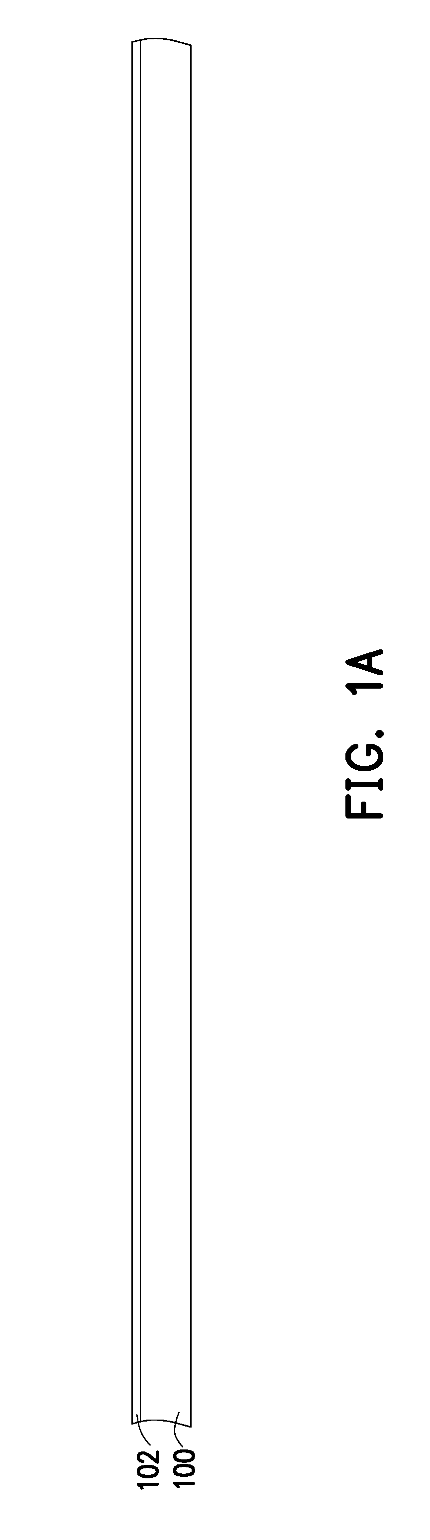
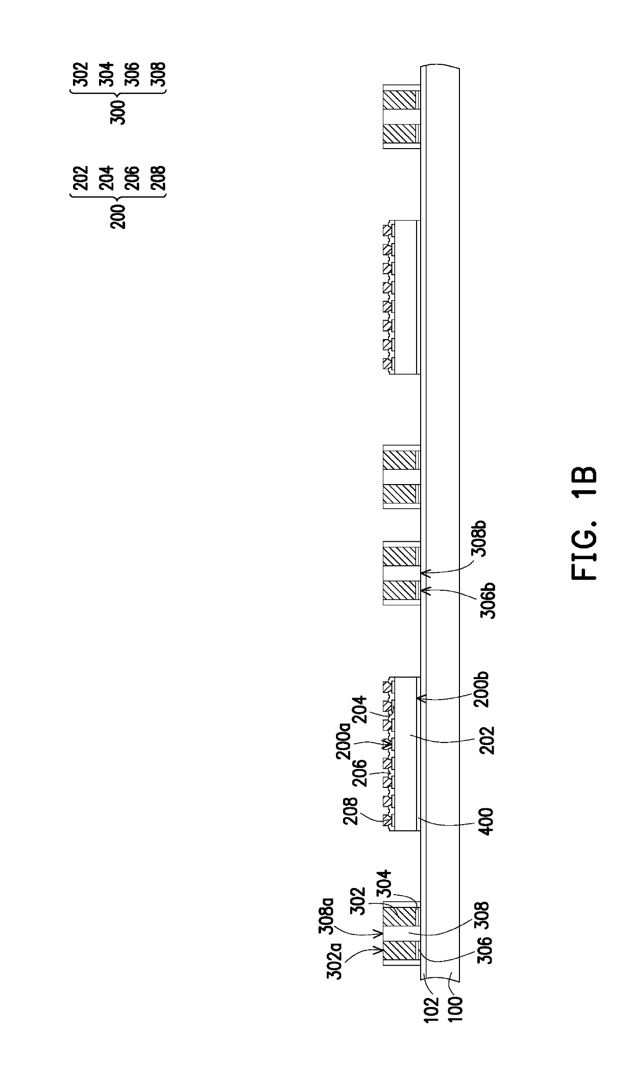
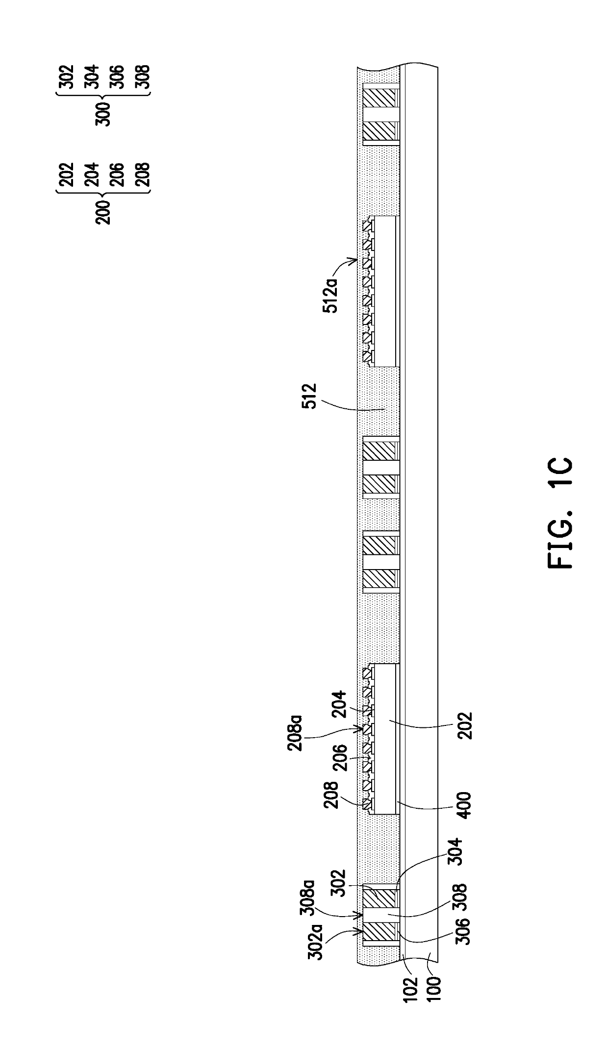
[0012]FIG. 1A to FIG. 1J are schematic cross-sectional views illustrating a manufacturing method of a package structure 10 according to some embodiments of the disclosure. Referring to FIG. 1A, a carrier 100 having a de-bonding layer 102 formed thereon is provided. The carrier 100 may be a glass substrate or a glass supporting board. However, they construe no limitation in the disclosure. Other suitable substrate material may be adapted as long as the material is able to withstand subsequent processes while structurally supporting the package structure formed thereon. The de-bonding layer 102 may include light to heat conversion (LTHC) materials, epoxy resins, inorganic materials, organic polymeric m...


PUM


Abstract

A package structure including a redistribution structure, a die, at least one connecting module, a first insulating encapsulant, a chip stack, and a second insulating encapsulant. The die is disposed on and electrically connected to the redistribution structure. The connecting module is disposed on the redistribution structure. The connecting module includes a protection layer and a plurality of conductive bars embedded in the protection layer. The first insulating encapsulant encapsulates the die and the connecting module. The chip stack is disposed on the first insulating encapsulant and the die. The chip stack is electrically connected to the connecting module. The second insulating encapsulant encapsulates the chip stack.

Description

CROSS REFERENCE TO RELATED APPLICATION[0001]This application claims the priority benefit of U.S. provisional application Ser. No. 62 / 591,166, filed on Nov. 27, 2017. The entirety of the above-mentioned patent application is hereby incorporated by reference herein and made a part of specification.BACKGROUND OF THE INVENTIONField of the Invention[0002]The disclosure generally relates to a package structure and a manufacturing method thereof, and in particular, to a package structure having a connecting module and a manufacturing method thereof.Description of Related Art[0003]Development of semiconductor package technology in recent years has focused on delivering products with smaller volume, lighter weight, higher integration level, and lower manufacturing cost. For multi-functional semiconductor packages, a technique for stacking chips has been used to provide the packages with a larger capacity to store or process data. The rapid increase in demand for multi-functional electronic c...

Claims


Application Information

Patent Timeline
Patent Type & Authority Applications(United States)
IPC IPC(8): H01L25/00H01L25/18H01L25/065H01L23/00H01L21/56H01L21/48
CPCH01L25/50H01L25/18H01L25/0657H01L24/73H01L21/561H01L21/568H01L21/4857H01L21/486H01L2225/06548H01L2225/0651H01L2225/06562H01L2224/73215H01L2224/73265H01L23/3107H01L23/3128H01L21/56H01L21/6835H01L2221/68318H01L2221/68359H01L2221/68372H01L2221/68381H01L24/45H01L2224/32145H01L2224/45124H01L2224/45144H01L2224/48091H01L2224/48145H01L2224/48227H01L2924/181H01L24/19H01L24/20H01L2221/68345H01L2224/73267H01L24/97H01L2224/02371H01L2224/49052H01L24/48H01L24/49H01L2224/48235H01L2224/83191H01L24/83H01L24/32H01L24/85H01L2224/73204H01L23/5389H01L23/49816H01L25/03H01L2225/06558H01L2225/06506H01L2924/00014H01L2224/32225H01L2924/00012H01L2224/16225H01L23/3135H01L23/528H01L24/06H01L21/563H01L21/76843H01L23/3157H01L23/562H01L24/09H01L24/17H01L23/5226H01L2224/02372
Inventor CHANG CHIEN, SHANG-YUHSU, HUNG-HSINLIN, NAN-CHUN
Owner POWERTECH TECHNOLOGY
Why Eureka
Try Eureka