Mems packaging structure and preparation method of mems packaging structure

A packaging structure and packaging circuit board technology, which is applied in the direction of sensors, electrical components, semiconductor electrostatic transducers, etc., can solve the problems of sensitivity and signal-to-noise ratio reduction, unfavorable product miniaturization, and large packaging size, etc., to improve sensitivity and Signal-to-noise ratio, small package size, and performance-enhancing effects

Active Publication Date: 2021-08-27
FOREHOPE ELECTRONICS NINGBO CO LTD
View PDF0 Cites 0 Cited by
  • Summary
  • Abstract
  • Description
  • Claims
  • Application Information

AI Technical Summary

Problems solved by technology

[0003] Existing MEMS silicon mic products have a large package size, which is not conducive to the miniaturization of the product. At the same time, the existing silicon mic products usually only adopt a single-sound cavity design, and the sound comes from a single hole / single direction (back sound input / front sound input) Sound), into the MEMS chip and metal cover, when the sound signal is very weak, the sound pressure signal is weaker, resulting in MEMS silicon wheat products, sensitivity and signal-to-noise ratio decline

Method used


Image

  • Mems packaging structure and preparation method of mems packaging structure
  • Mems packaging structure and preparation method of mems packaging structure
  • Mems packaging structure and preparation method of mems packaging structure

Examples


no. 1 example

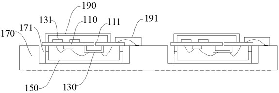
[0044] see figure 1 , the present invention provides a MEMS packaging structure 100, which can reduce the packaging size of silicon wheat products, is conducive to the miniaturization of silicon wheat products, and can realize the improvement of sensitivity and signal-to-noise ratio at the same time, so as to improve product performance, and can avoid When the sound pressure changes greatly, it will cause the rupture of the silicon diaphragm and play a good role in protecting the wiring structure.

[0045] The MEMS packaging structure 100 provided in this embodiment includes an integrated circuit board 110, a MEMS chip 130, a first cavity cover 150, a packaging circuit board 170 and a second cavity cover 190, and the MEMS chip 130 is mounted on the lower side of the integrated circuit board 110, The first cavity cover 150 is also mounted on the lower side of the integrated circuit board 110 and is covered outside the MEMS chip 130. The package circuit board 170 is provided wit...

no. 2 example

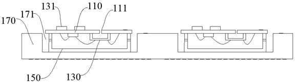
[0064] see figure 2 , this embodiment provides a MEMS package structure 100, its basic structure and principle and the technical effects produced are the same as those of the first embodiment, for a brief description, the parts not mentioned in this embodiment can refer to the first embodiment corresponding content. The difference between this embodiment and the first embodiment lies in the structure of the third chamber cover 191 .

[0065]In this embodiment, the MEMS package structure 100 includes an integrated circuit board 110, a MEMS chip 130, a first cavity cover 150, a packaging circuit board 170 and a second cavity cover 190, and the MEMS chip 130 is mounted on the lower side of the integrated circuit board 110, The first cavity cover 150 is also mounted on the lower side of the integrated circuit board 110 and is covered outside the MEMS chip 130. The package circuit board 170 is provided with a sound inlet accommodation groove 171, and the first cavity cover 150 is...

no. 3 example

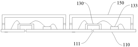
[0072] see image 3 , this embodiment provides a MEMS package structure 100, its basic structure and principle and the technical effects produced are the same as those of the first embodiment, for a brief description, the parts not mentioned in this embodiment can refer to the first embodiment corresponding content. Different from the first embodiment, in this embodiment, an adhesive layer is used to replace the third cavity cover 191 .

[0073] The MEMS packaging structure 100 includes an integrated circuit board 110, a MEMS chip 130, a first cavity cover 150, a packaging circuit board 170 and a second cavity cover 190, the MEMS chip 130 is mounted on the lower side of the integrated circuit board 110, and the first cavity cover 150 is also Mounted on the lower side of the integrated circuit board 110 and covered outside the MEMS chip 130, the packaging circuit board 170 is provided with a sound inlet accommodation groove 171, the first chamber cover 150 is correspondingly a...


PUM


Abstract

Embodiments of the present invention provide a MEMS packaging structure and a method for preparing the MEMS packaging structure, which relate to the field of chip packaging technology, and the MEMS packaging structure includes an integrated circuit board, a MEMS chip, a first chamber cover, a packaging circuit board and a second chamber cover. By opening the sound-inlet accommodation groove, the first chamber cover can be accommodated in the sound-inlet accommodation groove, which reduces the overall package height, further reduces the package volume, and is beneficial to the miniaturization of the product. At the same time, the first cavity cover is used as the front sound cavity of the MEMS chip to guide the transmission of sound pressure, and to prevent the external sound pressure from directly contacting the silicon diaphragm on the MEMS chip, thereby reducing the risk of silicon diaphragm rupture. At the same time, the second cavity cover is used as the MEMS The rear sound cavity of the chip improves the air space on the back of the MEMS chip, thereby improving the sensitivity and signal-to-noise ratio of the MEMS chip, and at the same time improving the frequency response of the MEMS chip.

Description

technical field [0001] The invention relates to the technical field of chip packaging, in particular to a MEMS packaging structure and a method for preparing the MEMS packaging structure. Background technique [0002] A silicon microphone includes a MEMS (Micro Electro Mechanical System, Micro Electro Mechanical System) chip, and the MEMS chip includes a silicon diaphragm and a silicon back plate. Among them, the working principle of the MEMS chip is to use the pressure gradient generated by the sound change to deform the silicon diaphragm when it is disturbed by the sound pressure, and then change the capacitance value between the silicon diaphragm and the silicon back plate, thereby converting the sound pressure signal into voltage signal. [0003] Existing MEMS silicon mic products have a large package size, which is not conducive to the miniaturization of the product. At the same time, the existing silicon mic products usually only adopt a single-sound cavity design, an...

Claims


Application Information

Patent Timeline
Patent Type & Authority Patents(China)
IPC IPC(8): H04R31/00H04R19/00
CPCH04R19/005H04R31/00H04R31/003H04R2201/003
Inventor 何正鸿钟磊李利
Owner FOREHOPE ELECTRONICS NINGBO CO LTD
Why Eureka
Try Eureka