

Chip-on-glass array substrate of liquid crystal display device and method of fabricating the same
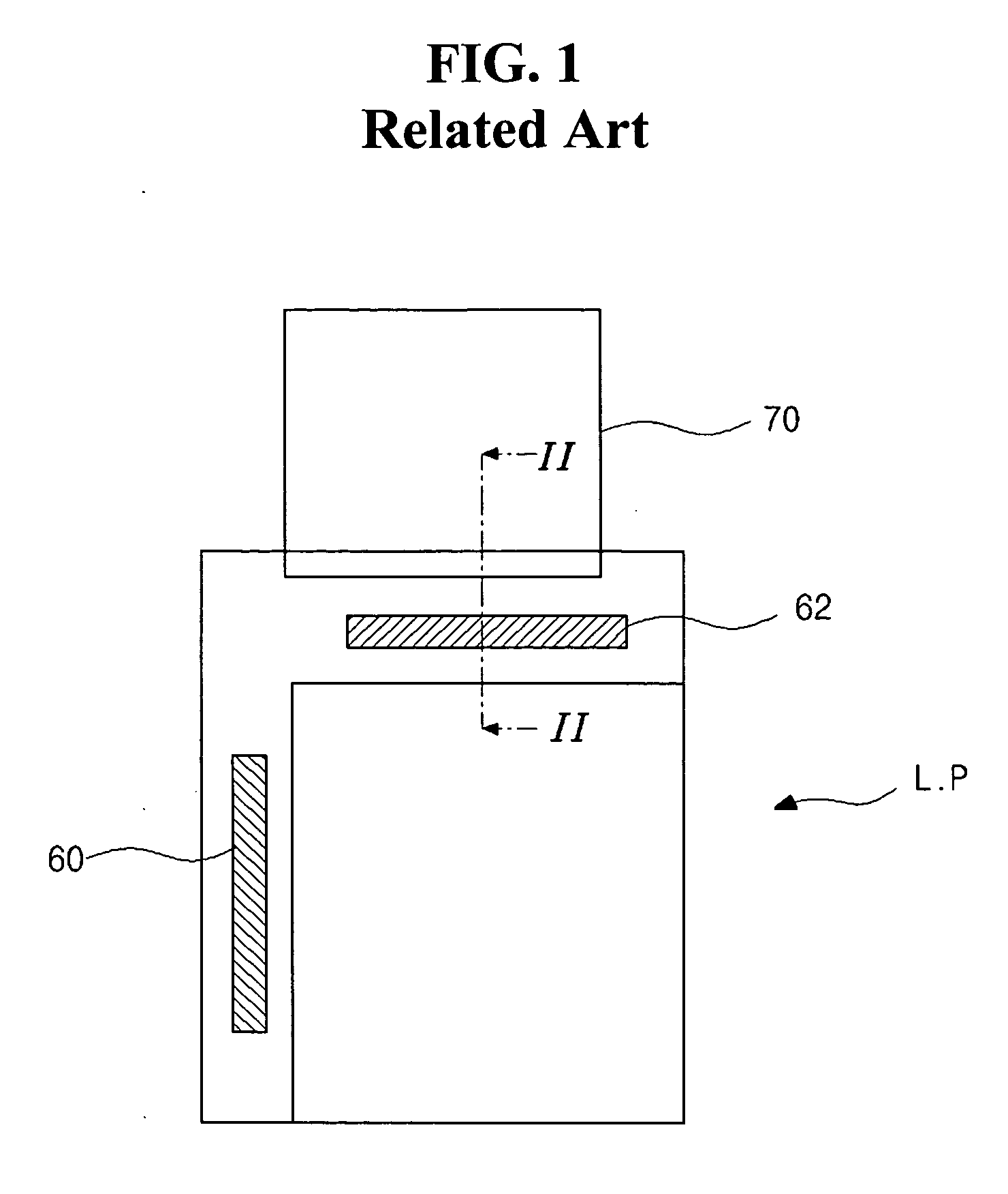
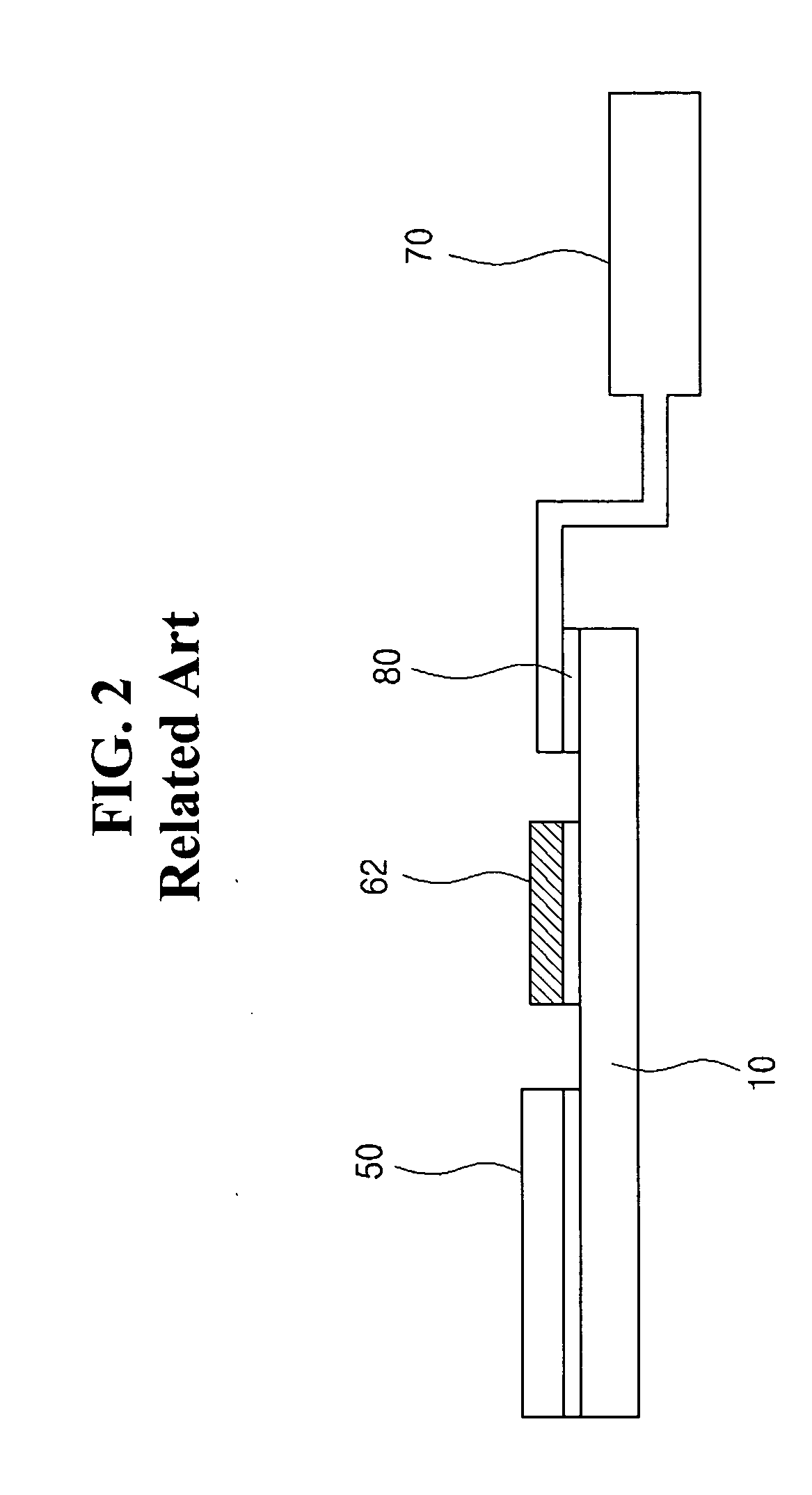
a liquid crystal display and array substrate technology, applied in non-linear optics, instruments, optics, etc., can solve the problems of creating an electrical open circuit condition, difficult to remove and repair defective drivers of driver ics or to repair terminal lines of lcd panels, and difficult to install driver ics on the pcb, so as to prevent damage, prevent damage, and stabilize the effect of ic chips
- Summary
- Abstract
- Description
- Claims
- Application Information
AI Technical Summary
Benefits of technology
Problems solved by technology
Method used
Image

Examples
Embodiment Construction
[0050] Reference will now be made in detail to preferred embodiments, examples of which are illustrated in the accompanying drawings.
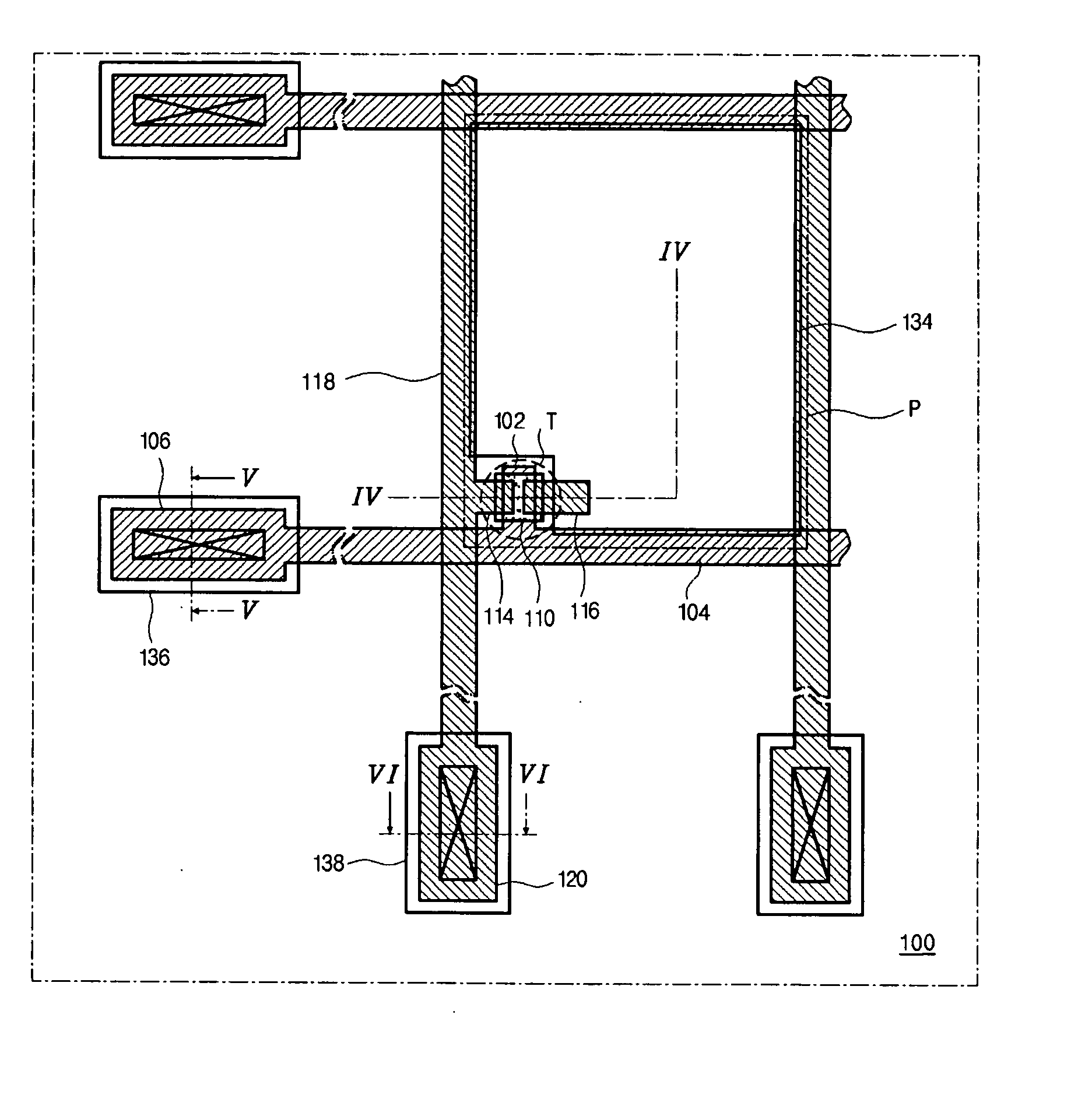
[0051]FIG. 9 is an enlarged plan view of an exemplary array substrate for an LCD device according to the present invention, FIGS. 10A-10G are cross sectional views along IV-IV of FIG. 9 of an exemplary method of fabricating an array substrate according to the present invention, FIGS. 11A-11G are cross sectional views along V-V of FIG. 9 of another exemplary method of an array substrate according to the present invention, FIGS. 12A-12G are cross sectional views along V-V of FIG. 9 of another exemplary method of fabricating an array substrate according to the present invention, and FIG. 13 is a cross sectional view along V-V of FIG. 9 of an exemplary gate pad region during application of an IC chip according to the present invention.
[0052] In FIGS. 10A, 11A, and 12A, a first metal layer may be deposited onto a surface of a substrate 100, and patterned ...
PUM
| Property | Measurement | Unit |
|---|---|---|
| dielectric constant | aaaaa | aaaaa |
| transparent | aaaaa | aaaaa |
| electrically conductive | aaaaa | aaaaa |
Abstract
Description
Claims
Application Information