

Methods of depositing materials over substrates, and methods of forming layers over substrates
a technology of materials and substrates, applied in the direction of chemically reactive gases, crystal growth processes, coatings, etc., can solve the problems of difficulty, difficulty, difficulty, difficulty, etc., and achieve the effect of speeding up pressure saturation
- Summary
- Abstract
- Description
- Claims
- Application Information
AI Technical Summary
Benefits of technology
Problems solved by technology
Method used
Image

Examples
Embodiment Construction
[0026] This disclosure of the invention is submitted in furtherance of the constitutional purposes of the U.S. Patent Laws “to promote the progress of science and useful arts” (Article 1, Section 8).
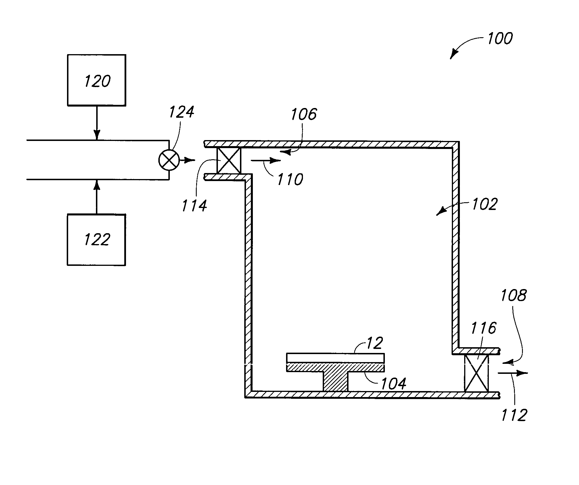
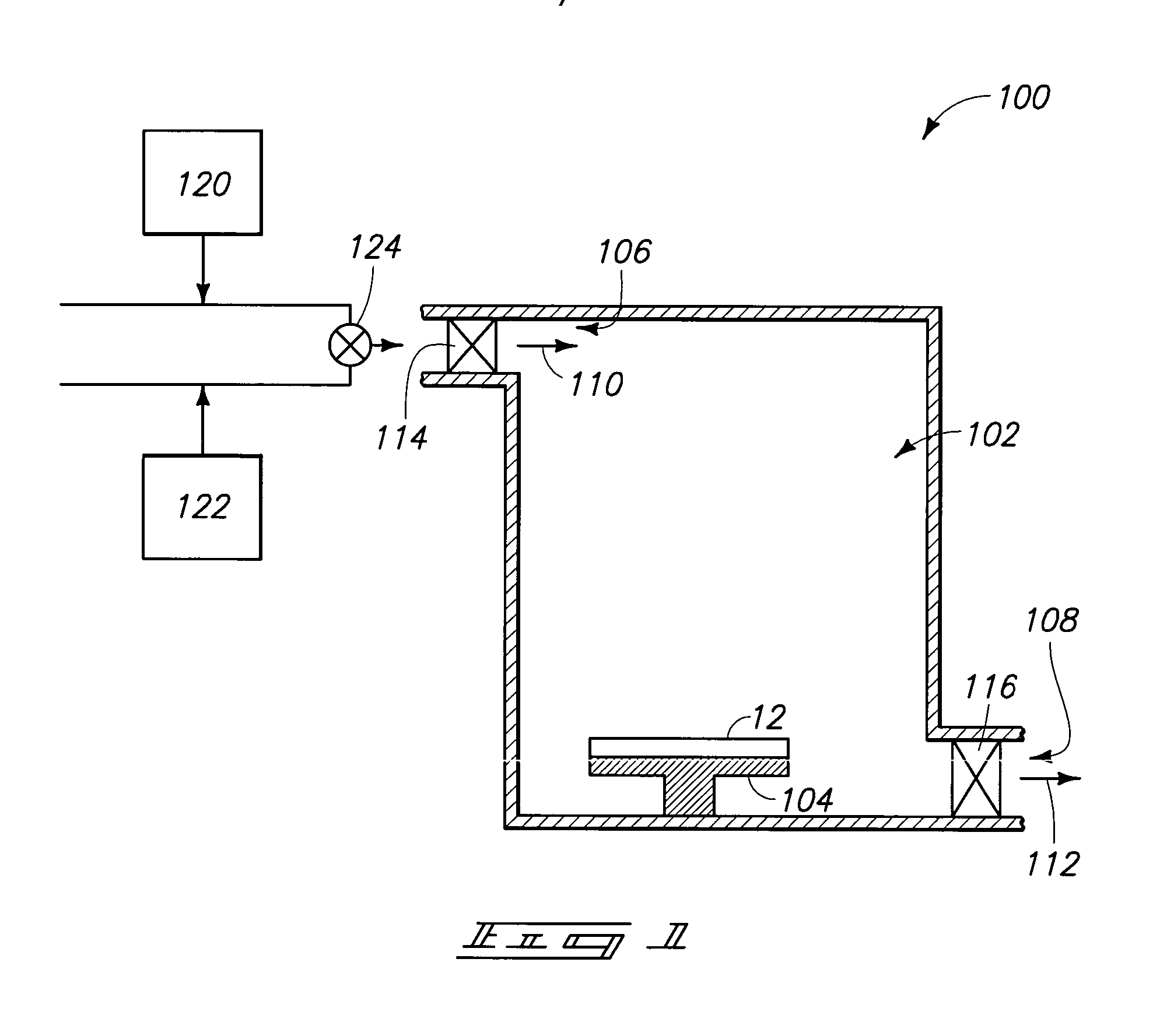
[0027] The invention includes various methods in which supercritical fluid is utilized to deliver one or more precursors into a reaction chamber during a deposition process. The supercritical fluid can be any suitable supercritical composition within which the precursor can be dispersed. Although the supercritical fluid can be a neat composition of precursor, typically it will not be. Instead, the supercritical fluid will comprise a composition other than that of the precursor, with an exemplary supercritical fluid being a supercritical fluid comprising, consisting essentially of, or consisting of carbon dioxide.
[0028] As is known to persons of ordinary skill in the art, a supercritical fluid is defined as any substance that is above its critical temperature (Tc) and critical pressure ...
PUM
| Property | Measurement | Unit |
|---|---|---|
| vapor pressure | aaaaa | aaaaa |
| critical temperature | aaaaa | aaaaa |
| critical pressure | aaaaa | aaaaa |
Abstract
Description
Claims
Application Information