Methods of forming particle-containing materials; and semiconductor constructions comprising particle-containing materials

a technology of particle-containing materials and semiconductors, which is applied in the direction of transportation and packaging, coatings, chemistry apparatuses and processes, etc., to achieve the effect of speeding up pressure saturation

Active Publication Date: 2005-06-02
MICRON TECH INC
View PDF16 Cites 13 Cited by
  • Summary
  • Abstract
  • Description
  • Claims
  • Application Information

AI Technical Summary

Benefits of technology

[0005] The first species is purged from over the substrate and a second chemical species is provided to chemisorb onto the first monolayer of the first species. The second species is then purged and the steps are repeated with exposure of the second species monolayer to the first species. In some cases, the two monolayers may be of the same species. Also, a third species or more may be successively chemisorbed and purged just as described for the first and second species. It is noted that one or more of the first, second and third species can be mixed with inert gas to speed up pressure saturation within a reaction chamber.

Problems solved by technology

Nevertheless, such an imperfect monolayer is still a monolayer in the context of this document.
The second species might only bond to the first species and thus may also be self-limiting.

Method used


Image

  • Methods of forming particle-containing materials; and semiconductor constructions comprising particle-containing materials
  • Methods of forming particle-containing materials; and semiconductor constructions comprising particle-containing materials
  • Methods of forming particle-containing materials; and semiconductor constructions comprising particle-containing materials

Examples


Embodiment Construction

[0028] This disclosure of the invention is submitted in furtherance of the constitutional purposes of the U.S. Patent Laws “to promote the progress of science and useful arts” (Article 1, Section 8).

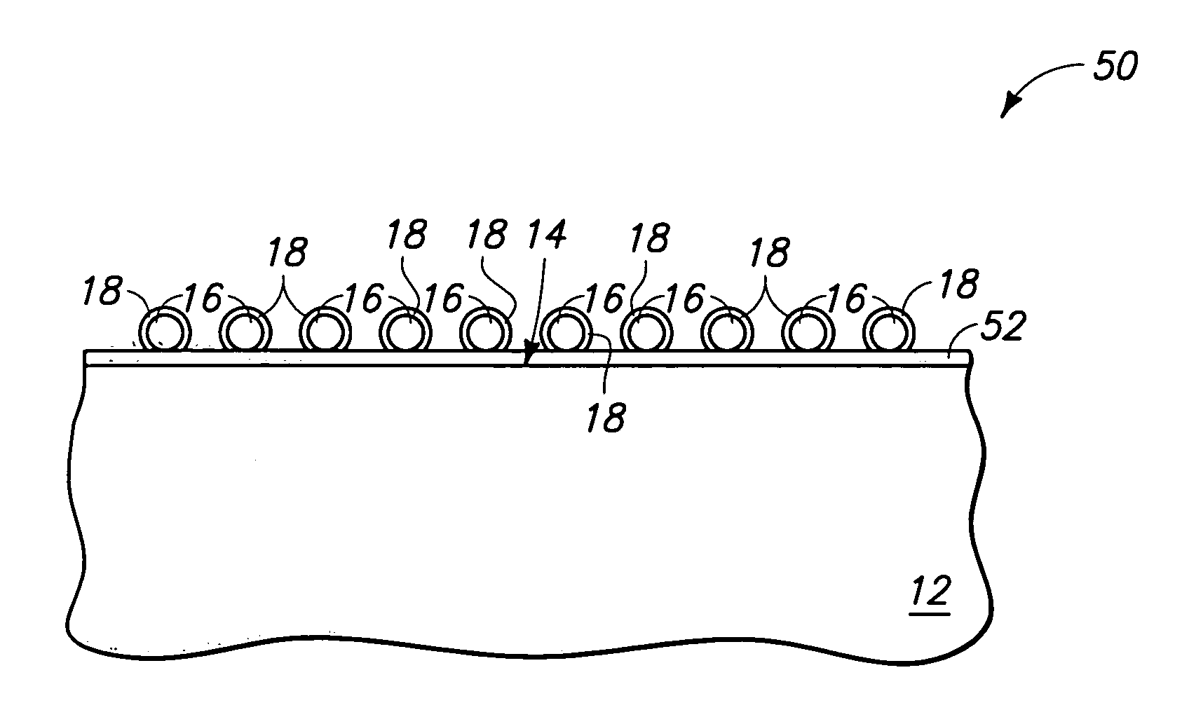
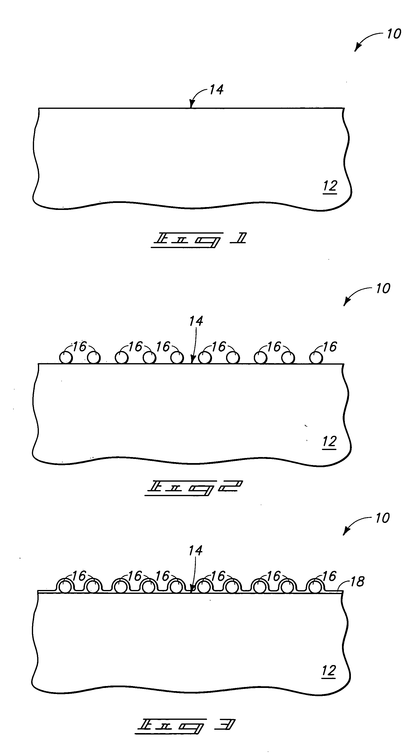
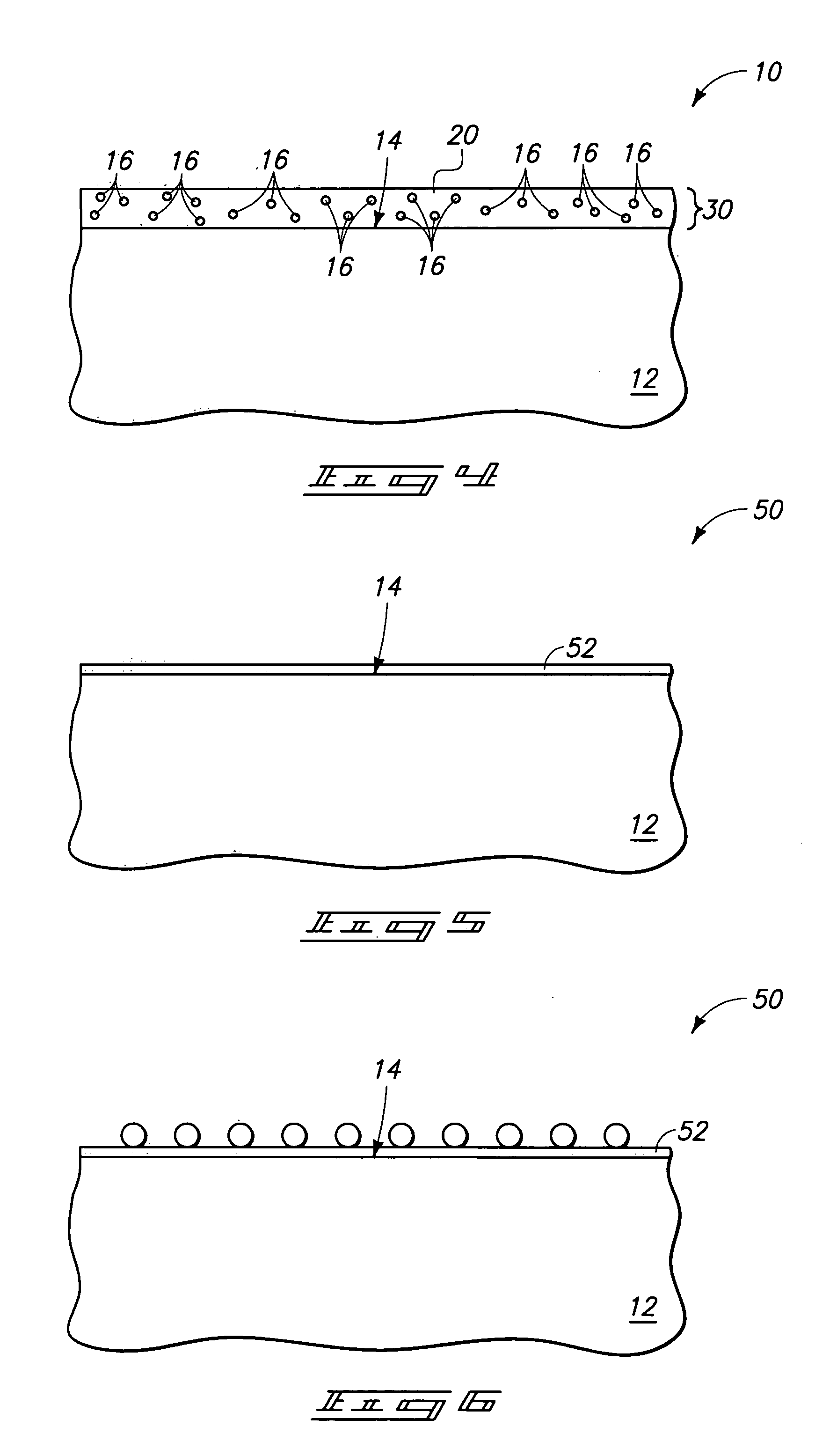
[0029] The invention includes methods by which particles can be incorporated into layers during semiconductor device fabrication. In particular aspects, the particles can have a size from about 100 Å to about 10,000 Å, and in specific aspects the particles can be so-called nanoparticles. The particles can be formed remotely from a semiconductor substrate and then transferred to the substrate. This can allow the particles to be formed in environments particularly well-suited to particle fabrication, and can also allow avoidance of exposure of the semiconductor substrate to the environments utilized for particle formation. The conditions utilized to form the particles can thus be established to be economically highly suited for particle formation. Also, the conditions utilized to form the...


PUM

PropertyMeasurementUnit
dimensionaaaaaaaaaa
electrically insulativeaaaaaaaaaa
K dielectricaaaaaaaaaa

Abstract

The invention includes methods of forming particle-containing materials, and also includes semiconductor constructions comprising particle-containing materials. One aspect of the invention includes a method in which a first monolayer is formed across at least a portion of a semiconductor substrate, particles are adhered to the first monolayer, and a second monolayer is formed over the particles. Another aspect of the invention includes a construction containing a semiconductor substrate and a particle-impregnated conductive material over at least a portion of the semiconductor substrate. The particle-impregnated conductive material can include tungsten-containing particles within a layer which includes tantalum or tungsten.

Description

TECHNICAL FIELD [0001] The invention pertains to methods of forming particle-containing materials, and also pertains to semiconductor constructions comprising particle-containing materials. BACKGROUND OF THE INVENTION [0002] Semiconductor device fabrication typically involves formation of multiple layers over a semiconductor substrate. Various methods are known which can be utilized to form the layers, with exemplary methods including atomic layer deposition (ALD), chemical vapor deposition (CVD), and physical vapor deposition (PVD). [0003] The present invention has particular application to ALD processes. ALD technology typically involves formation of successive atomic layers on a substrate. Such layers may comprise, for example, an epitaxial, polycrystalline, and / or amorphous material. ALD may also be referred to as atomic layer epitaxy, atomic layer processing, etc. [0004] Described in summary, ALD includes exposing an initial substrate to a first chemical species to accomplish c...

Claims


Application Information

Patent Timeline
Patent Type & Authority Applications(United States)
IPC IPC(8): B32B15/00H01L21/288H01L21/768
CPCC23C16/45525Y10T428/12576H01L21/02126H01L21/02164H01L21/0226H01L21/0228H01L21/288H01L21/3141H01L21/3146H01L21/31608H01L21/31633H01L21/76829H01L21/76837H01L21/76838Y10S438/964Y10S438/962Y10T428/12806Y10T428/1284Y10T428/12493Y10T428/12528C23C16/45555
Inventor DERDERIAN, GARO J.SANDHU, GURTEJ S.
Owner MICRON TECH INC
Why Eureka
Try Eureka