Solid-state imaging device and manufacturing method thereof

a technology of solid-state imaging and manufacturing methods, which is applied in the direction of color television, television systems, radio control devices, etc., can solve problems such as color mixing, and achieve the effect of preventing color mixing and reducing the variation in light sensitivity among pixels

Active Publication Date: 2005-03-03
COLLABO INNOVATIONS INC
View PDF2 Cites 29 Cited by
  • Summary
  • Abstract
  • Description
  • Claims
  • Application Information

AI Technical Summary

Benefits of technology

[0015] Therefore, an object of the present invention is to provide a solid-state imaging device capable of preventing color mixing caused by oblique light, and reducing variation in light sensitivity among pixels.

Problems solved by technology

However, the solid-state imaging device as shown in FIG. 8 has a problem that light entering the solid-state imaging device obliquely from above (hereinafter, referred to as oblique light) enters an adjacent pixel, whereby color mixing occurs.

Method used


Image

  • Solid-state imaging device and manufacturing method thereof
  • Solid-state imaging device and manufacturing method thereof
  • Solid-state imaging device and manufacturing method thereof

Examples


Embodiment Construction

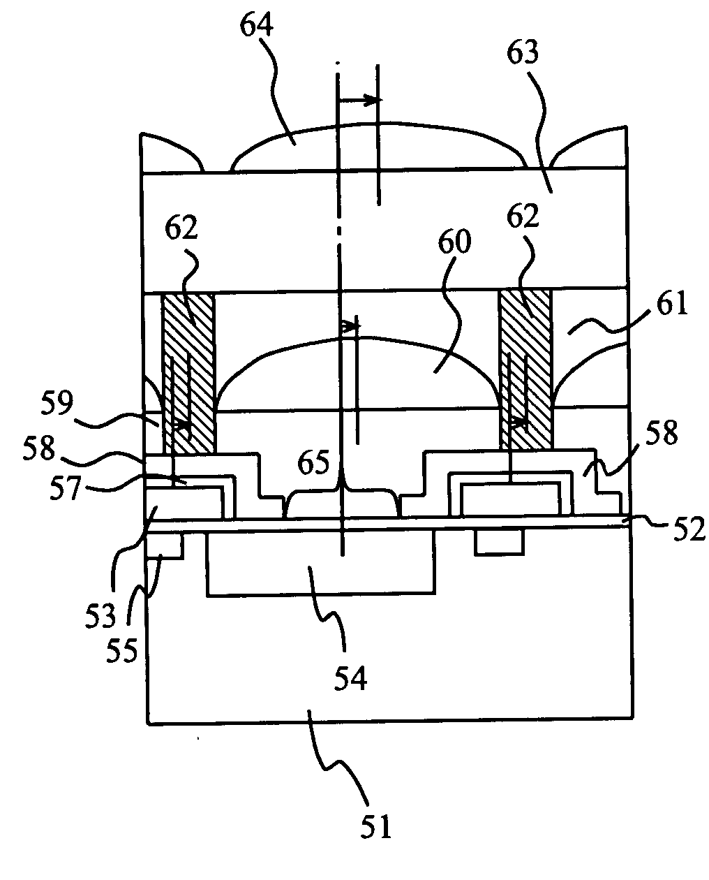
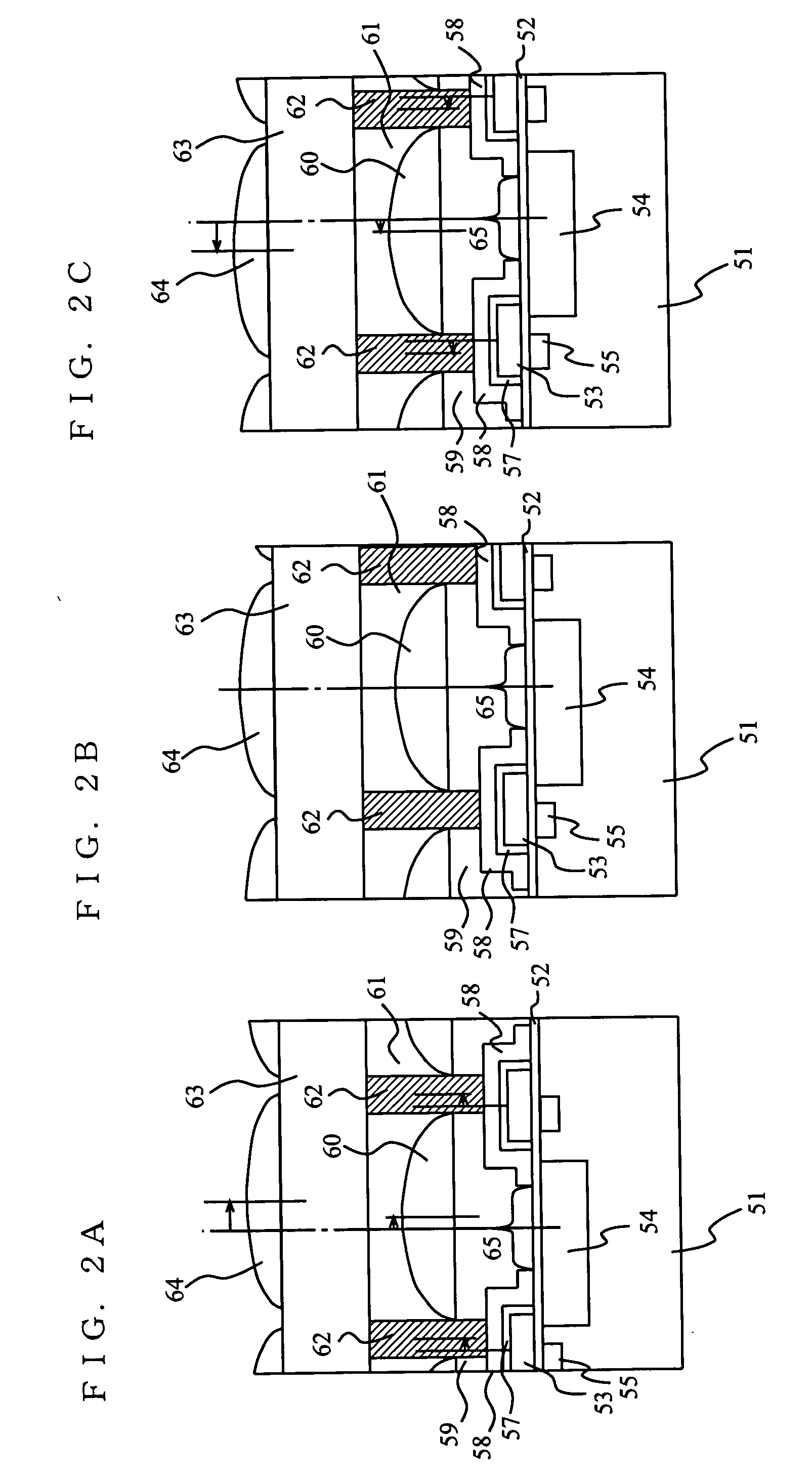
[0040] Hereinafter, with reference to the drawings, a solid-state imaging device according to one embodiment of the present invention will be described. FIG. 1 is an illustration showing a structure of the entirety of the solid-state imaging device according to the present embodiment. FIGS. 2A to 2C are cross section views of pixels located at the left edge, at the center, and at the right edge, respectively, of a photoreceiving region of the solid-state imaging device as shown in FIG. 1.

[0041] As shown in FIG. 1, the solid-state imaging device according to the present embodiment includes a light receiving section 1, a vertical CCD shift resistor 2, and a horizontal CCD shift resistor 3.

[0042] The light receiving section 1 includes a light-sensitive element such as a photodiode, and a plurality of the light receiving sections 1 are arranged in a matrix form at regular spacings in a rectangular photoreceiving region, as shown in FIG. 1. The light receiving section 1 generates a sig...


PUM


Abstract

The solid-state imaging device according to the present invention comprises: a plurality of light-sensitive elements 1 arranged in a matrix form at regular spacings in a photoreceiving region provided on a semiconductor substrate; a plurality of detecting electrodes provided on the semiconductor substrate corresponding to the plurality of the light-sensitive elements for detecting an electrical charge generated by each light-sensitive element; a light-shielding film 58 coating the plurality of detecting electrodes and having an aperture 65 over each light-sensitive element; and a plurality of reflecting walls 62, which are formed in a grid pattern over the light-shielding film so as to partition the apertures individually over the respective light-sensitive elements, for reflecting a portion of light entering the semiconductor substrate from above onto the aperture on each light-sensitive element. The plurality of reflecting walls are formed so that a middle point of the reflecting walls opposing each other across the aperture is displaced from a center of the aperture toward a center of the photoreceiving region.

Description

BACKGROUND OF THE INVENTION [0001] 1. Field of the Invention [0002] The present invention relates to a solid-state imaging device. More particularly, the present invention relates to a solid-state imaging device in which a plurality of light-sensitive elements are arranged in a matrix form. [0003] 2. Description of the Background Art [0004] In order to improve the light collecting power of a solid-state imaging device typified by a CCD, there exists a solid-state imaging device in which two micro lenses are formed as shown in FIG. 8. Hereinafter, with reference to FIG. 8, the above-described solid-state imaging device will be described. [0005] The solid-state imaging device as shown in FIG. 8 includes a semiconductor substrate 501, a gate insulating film 502, a gate electrode 503, a photodiode 504, a charge transfer section 505, an interlayer insulating film 507, a light-shielding film 508, an insulating film 509, an intralayer lens 510, a planarization film 511, a color filter 513,...

Claims


Application Information

Patent Timeline
Patent Type & Authority Applications(United States)
IPC IPC(8): H01L27/14H01L21/00H01L27/146H01L27/148H01L31/02H01L31/0216H01L31/0232H01L31/062H04N5/225H04N5/335H04N5/365H04N5/369H04N5/372
CPCH01L27/1463H01L27/14685H01L27/14818H01L27/14629H01L31/0232H01L27/14621H01L27/14625H01L31/02164H01L27/14605H01L31/02325
Inventor KURIYAMA, TOSHIHIRO
Owner COLLABO INNOVATIONS INC
Why Eureka
Try Eureka