Digital delay elements constructed in a programmable logic device

Inactive Publication Date: 2005-03-03
NATIONAL INSTRUMENTS
View PDF18 Cites 65 Cited by
  • Summary
  • Abstract
  • Description
  • Claims
  • Application Information

AI Technical Summary

Benefits of technology

[0008] In one embodiment, each of the one or more delay circuits includes delay elements having a large delay, delay elements having a medium delay, and delay elements having a fine delay. The large delay elements may include inverters and/or non-inverting buffers, and provide delay step sizes that are coarse with respect to the medium and fine delay elements. The medium delay elements may include an inverter or a non-inverting buffer, and provide a delay step size that is less than that of a large delay element but greater than that provided by a fine

Problems solved by technology

In complex digital systems, there often exists a need to adjust the phase delay of one or more signals.
These independent components can consume valuable board area.
Such delay line components may be expensive and have fixed functionality (e.g., the range and resolution of the delay is set by the vendor and is not configurable).
Given their expense, their lack

Method used


Image

  • Digital delay elements constructed in a programmable logic device
  • Digital delay elements constructed in a programmable logic device
  • Digital delay elements constructed in a programmable logic device

Examples


Embodiment Construction

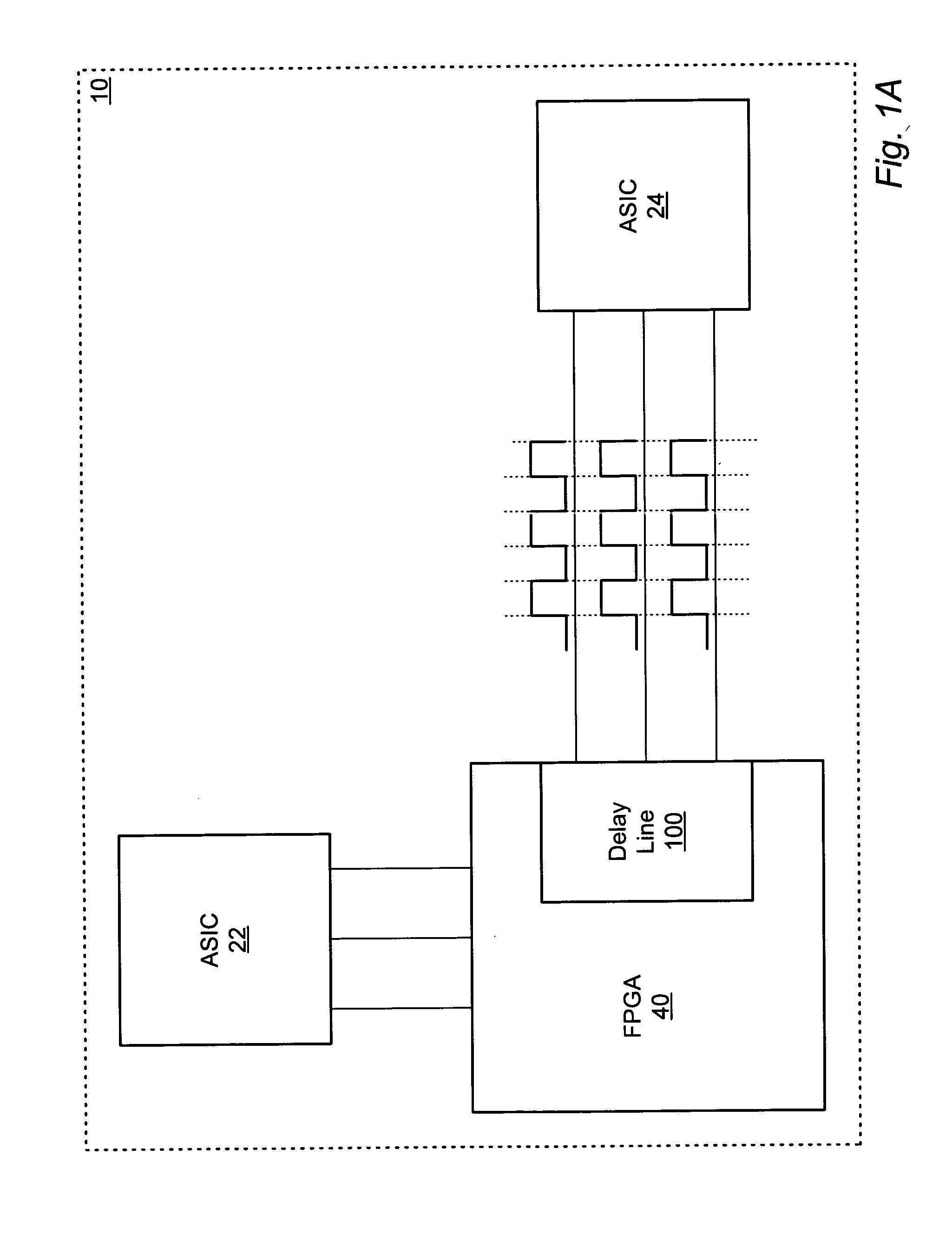
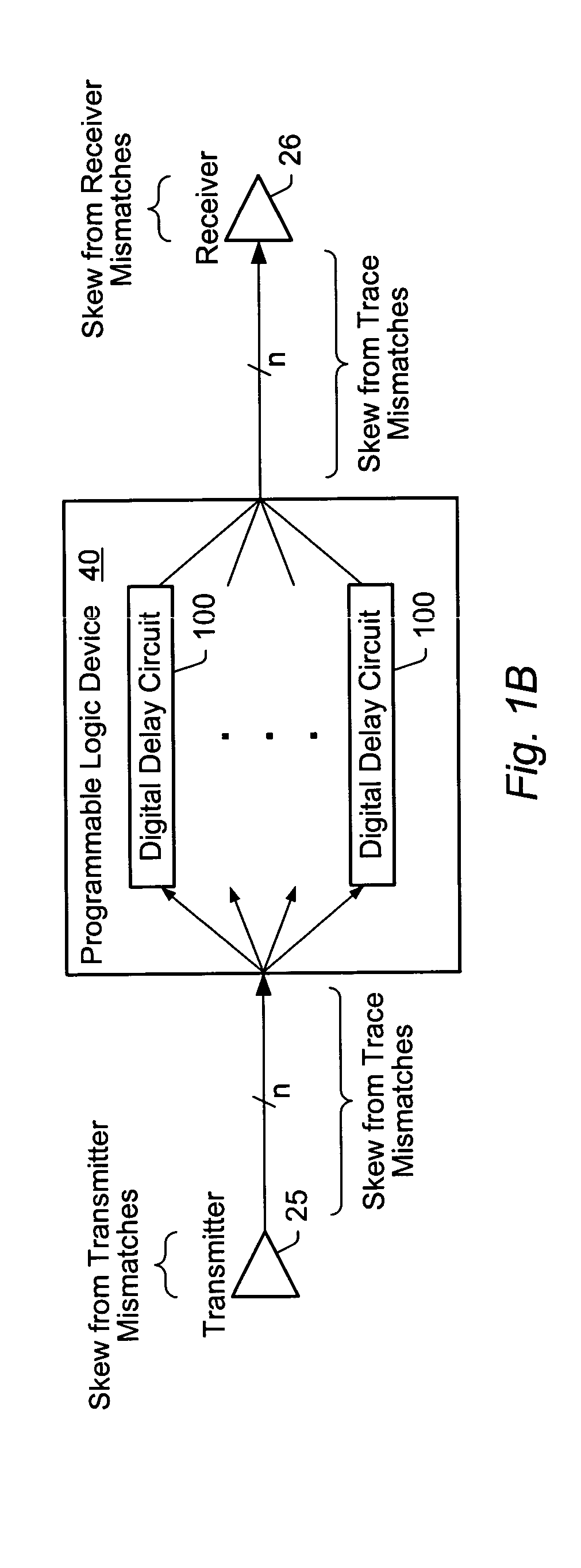
[0022] Turning now to FIG. 1A, a block diagram of one embodiment of an exemplary system implementing delay lines using a programmable logic device is shown. System 10 is an exemplary electronic system which includes application specific integrated circuits (ASIC's) 22 and 24, both of which are coupled to field programmable gate array (FPGA) 40. FPGA 40 is a programmable logic device (PLD) that is configured to perform various functions of system 10. Other types of PLD's may be used in lieu of FPGA 40.

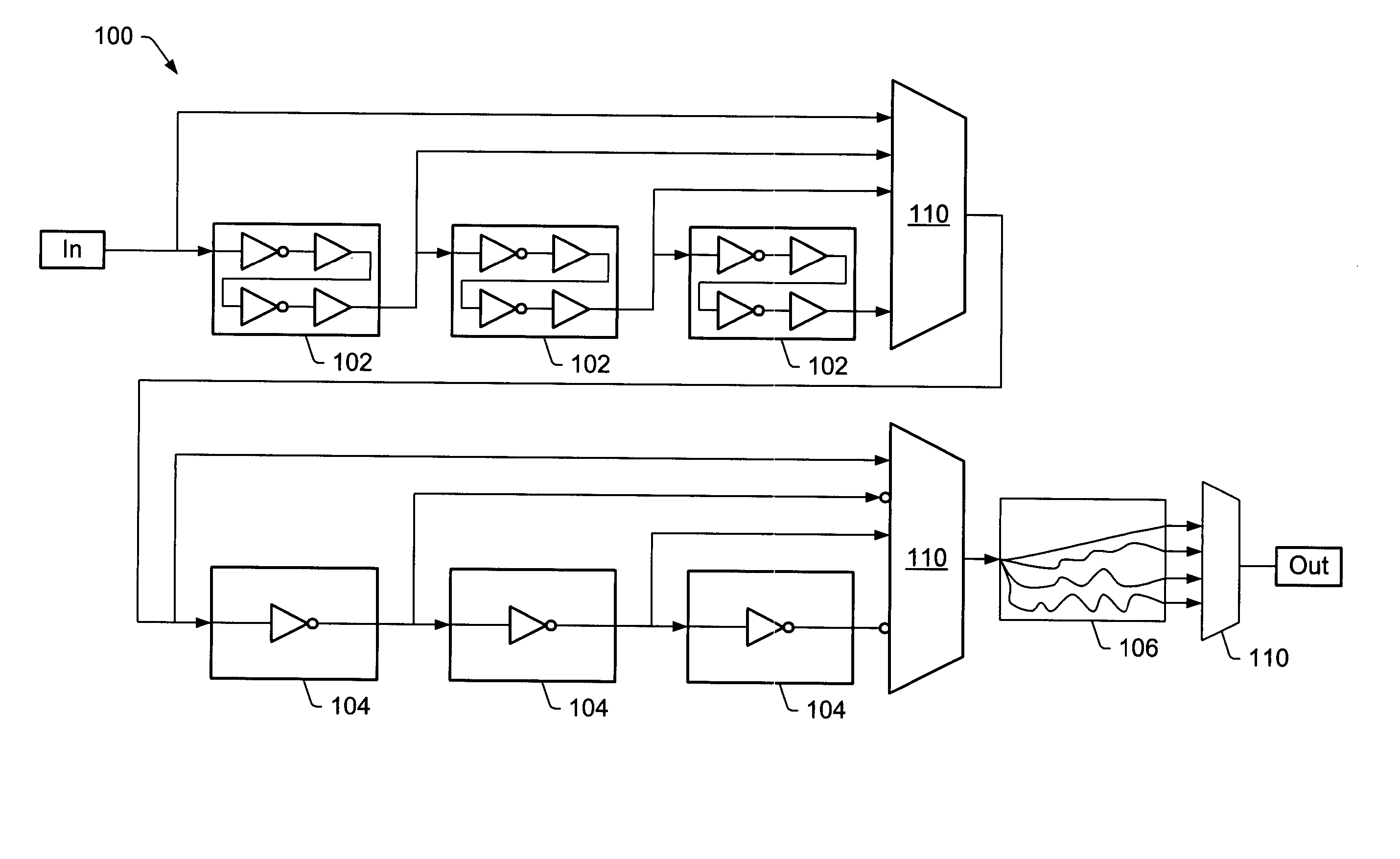
[0023] Delay circuit 100 is implemented in FPGA 40, and is configured to provide delay to signals being transmitted to ASIC 24, and may be one of a plurality of delay circuit implemented in FPGA 40. Delay circuit 100 may be configured during the programming of FPGA 40. The configuring of delay circuit 100 may be done with several specific objectives in mind.

[0024] One objective is to configure delay circuit 100 such that it has a certain resolution, which is the amount of delay per st...


PUM


Abstract

A delay circuit. In one embodiment, a programmable logic device (PLD) is used to implement one or more delay circuits having a plurality of delay elements. Included in the plurality of elements are a balanced number of logic elements such that rising and falling edges of a signal passing through the delay circuit propagate with substantially the same amount of delay. The delay circuit may also include a selector circuit coupled to select an output from one of the plurality of delay elements. The delay circuit may be implemented such that it preserves the duty cycle and/or pulse width of signals to which the delay is applied.

Description

BACKGROUND OF THE INVENTION [0001] 1. Field of the Invention [0002] This invention relates to digital circuits, and more particularly, the delay lines implemented in digital circuits. [0003] 2. Description of the Related Art [0004] In complex digital systems, there often exists a need to adjust the phase delay of one or more signals. The phase delay of signals may need to be adjusted for clock and / or data alignment purposes, and may be necessary to ensure that data being transmitted or received is properly synchronized with a clock signal. For example, a plurality of signals transmitted in parallel on a bus may be required to arrive at a receiver at approximately the same time. Such timing is especially critical for digital systems that operate at high frequencies. [0005] One common method of adjusting the phase delay of signals in a digital system is to use delay lines. Delay lines may be implemented as independent components. These independent components can consume valuable board...

Claims


Application Information

Patent Timeline
IPC IPC(8): G06F1/10G06F1/12H03H11/26H03K5/00H03K5/13
CPCG06F1/10H03K2005/00156H03K5/133G06F1/12
Inventor SCHROEDER, CHARLES G.BAKER, DANIEL J.SESCILA, GLEN O. III
Owner NATIONAL INSTRUMENTS
Why Eureka
Try Eureka