
Switching activity reduced coding for low-power digital signal processing circuitry

Inactive Publication Date: 2005-03-03
AVAGO TECH WIRELESS IP SINGAPORE PTE
View PDF4 Cites 3 Cited by
  • Summary
  • Abstract
  • Description
  • Claims
  • Application Information

AI Technical Summary

Benefits of technology

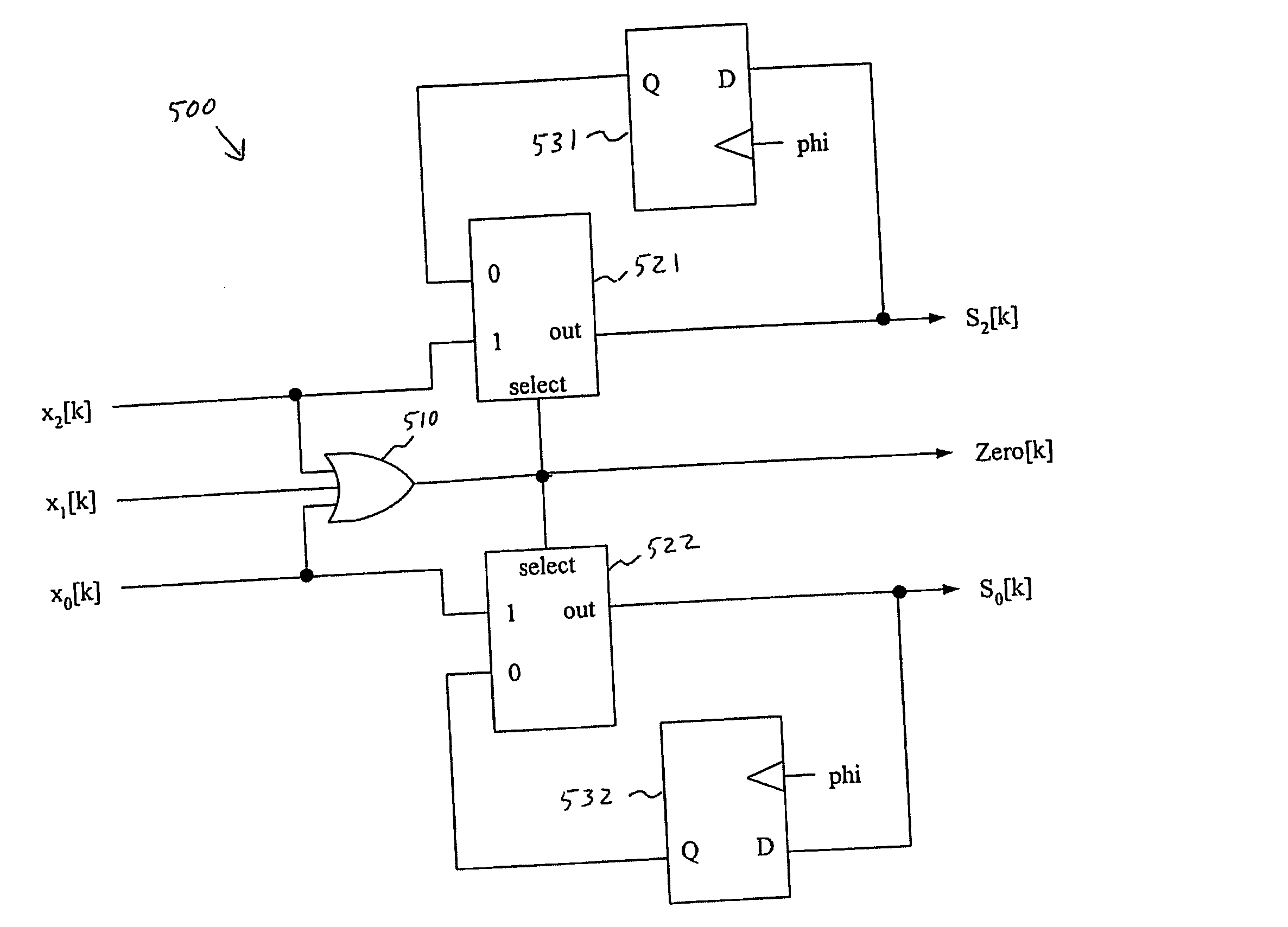
[0011] A system and method are provided for reducing power consumption in digital signal processing circuitry by reducing the amount of unnecessary switching in such circuitry. An aspect of the present invention includes a switching-reduction circuit that may include an output sub-circuit outputting a current output signal to a subsequent digital signal processing circuit. The switching-reduction circuit may also include a logic sub-circuit that receives a next input signal and determines whether the next input signal is relevant to a next output of the subsequent digital signal processing circuit. If the next input signal may be relevant to the next output of the subsequent digital signal processing circuit, the logic sub-circuit causes the output sub-circuit to output the next input signal to the subsequent digital signal processing circuit. If, however, the next input signal will not be relevant to the next output of the subsequent digital signal processing circuit, the logic sub-circuit causes the output sub-circuit to output again the current output signal to the subsequent digital signal processing circuit.
[0012] Another aspect of the present invention provides a method for reducing unnecessary switching in a subsequent digital circuit. The method may include outputting a current output signal to the subsequent digital circuit. The method may further include receiving a next input signal and determining, based on anticipated behavior of the subsequent digital circuit, whether the next input signal will be relevant to the next output of the subsequent digital circuit. If the next input signal may be relevant to the next output of the subsequent digital circuit, the method may include outputting the next input signal to the subsequent digital circuit. If, however, the next input signal will not be relevant to the next output of the subsequent digital circuit, the method may include outputting again the current output signal to the subsequent digital circuit.

Problems solved by technology

Power consumption is a primary concern in many modern electrical circuits.
Power consumption may limit the extent to which a circuit may be reduced in size.
Power consumption limits the amount of time a portable device may operate with a limited supply of power.
Such solutions often result in circuits with fewer devices, which often corresponds with lower power consumption.
A problem with many, if not all, of such digital signal processing circuits is that the circuits perform unnecessary switching.
Further, unnecessary switching not only results in unnecessary power consumption, but also results in unnecessary device wear and reduced life, thereby providing further incentive to develop methods and apparatus that reduce the amount of unnecessary switching in digital signal processing circuitry.

Method used


Image

  • Switching activity reduced coding for low-power digital signal processing circuitry
  • Switching activity reduced coding for low-power digital signal processing circuitry
  • Switching activity reduced coding for low-power digital signal processing circuitry

Examples


Embodiment Construction

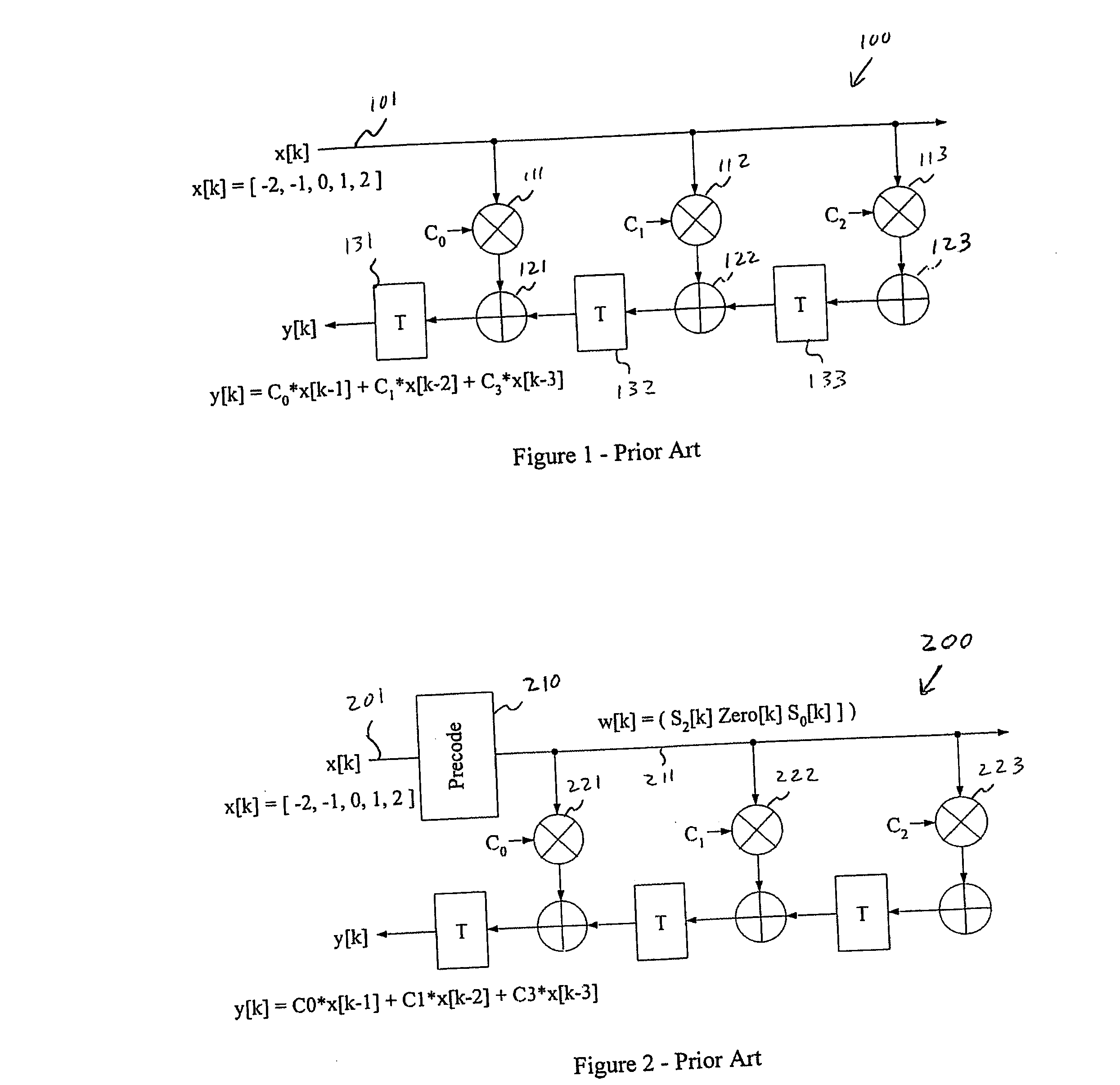
[0023]FIG. 1 is a diagram illustrating a traditional Finite Impulse Response (FIR) filter 100 in transposed form. The illustrated FIR filter 100 shows only three taps, but FIR filters may typically have a large number of taps. The input signal 101 (or “x”) arrives at first, second and third coefficient multipliers 111-113, which multiply the input signal 101 by respective filter coefficients C0, C1 and C2. A third adder circuit 123 adds the output of the third coefficient multiplier 113 to the results from further filter taps 125, not illustrated, which for this example are set to zero. A third delay element 133 receives the output of the third adder circuit 123 and delays the output of the third adder circuit 123 by one sample period.

[0024] A second adder circuit 122 adds the output of the second coefficient multiplier 112 to the output of the third delay element 133. A second delay element 132 receives the output of the second adder circuit 122 and delays, by one sample period, t...


PUM


Abstract

A system and method for reducing power consumption in digital circuitry by reducing the amount of unnecessary switching in such circuitry. An aspect of the present invention provides a switching-reduction circuit that outputs a signal to a subsequent digital circuit. The value of the signal may depend on the relevance of the signal value to a next output of the subsequent digital circuit. A method according to various aspects of the present invention includes receiving a next input signal. The method further includes determining whether the next input signal may be relevant to a next output of a subsequent digital circuit. The method further includes providing the next input signal to the subsequent digital circuit when the next input signal may be relevant to the next output of the subsequent digital circuit, and providing a previous signal to the subsequent digital circuit when the next input signal will not be relevant to the next output of the subsequent digital circuit.

Description

CROSS-REFERENCE TO RELATED APPLICATIONS / INCORPORATION BY REFERENCE [0001] [Not Applicable]FEDERALLY SPONSORED RESEARCH OR DEVELOPMENT [0002] [Not Applicable][SEQUENCE LISTING][0003] [Not Applicable][MICROFICHE / COPYRIGHT REFERENCE][0004] [Not Applicable]FIELD OF THE INVENTION [0005] The present invention relates generally to reducing power consumption in digital circuitry. The present invention relates more specifically to using intelligent pre-coding to reduce switching, and therefore power consumption, in digital signal processing circuitry. BACKGROUND OF THE INVENTION [0006] Power consumption is a primary concern in many modern electrical circuits. A primary goal with many circuits is to make them as small as possible. Power consumption may limit the extent to which a circuit may be reduced in size. Another primary goal with many electrical circuits is to make circuits that can run longer with a limited supply of power, such as in portable products like cellular phones and portabl...

Claims


Application Information

Patent Timeline
IPC IPC(8): G06F7/52G06F7/533H03H17/02
CPCG06F7/533H03H2017/0692H03H17/0236G06F7/5336
Inventor LUTKEMEYER, CHRISTIAN
Owner AVAGO TECH WIRELESS IP SINGAPORE PTE
Learn More