

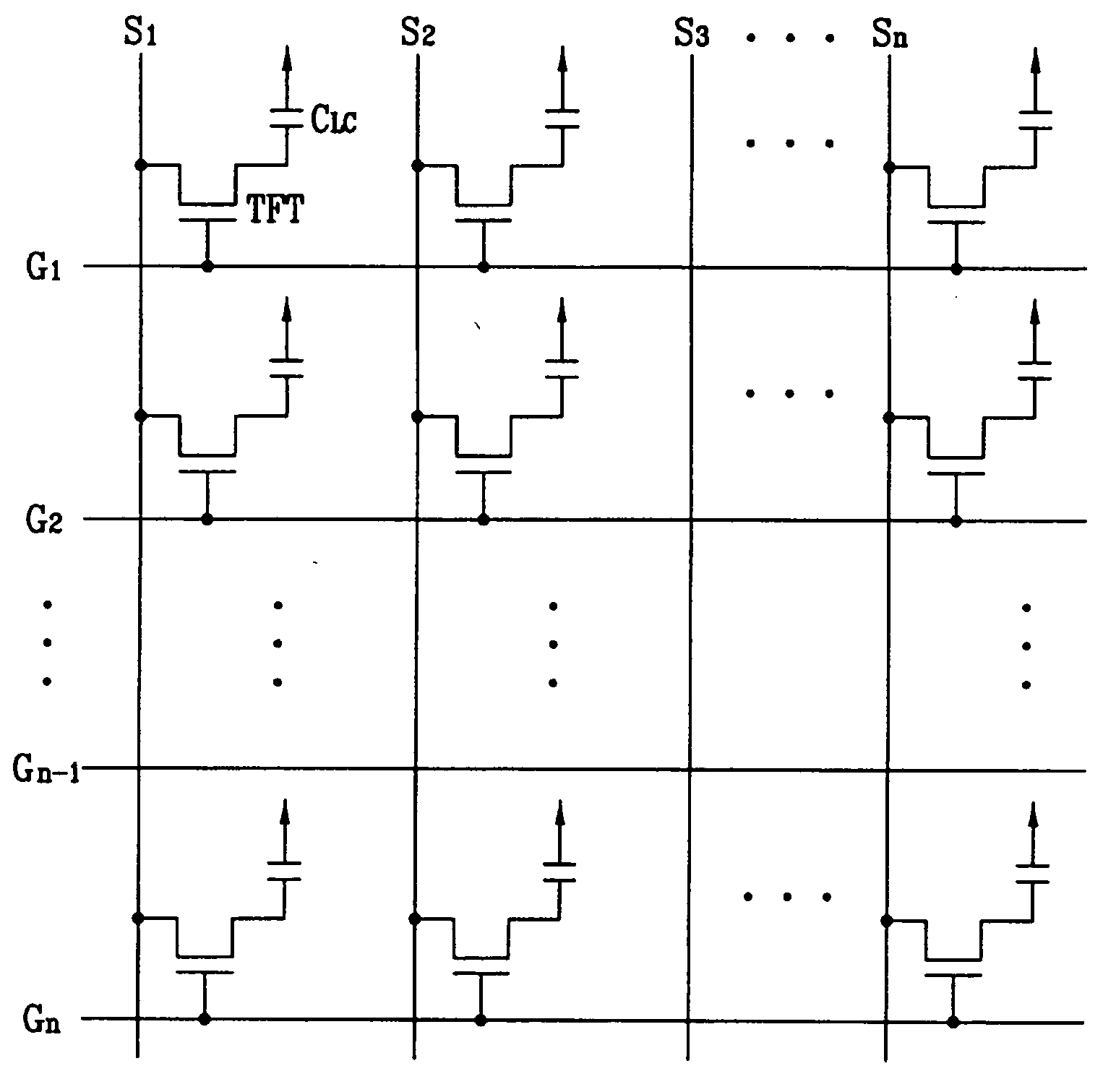
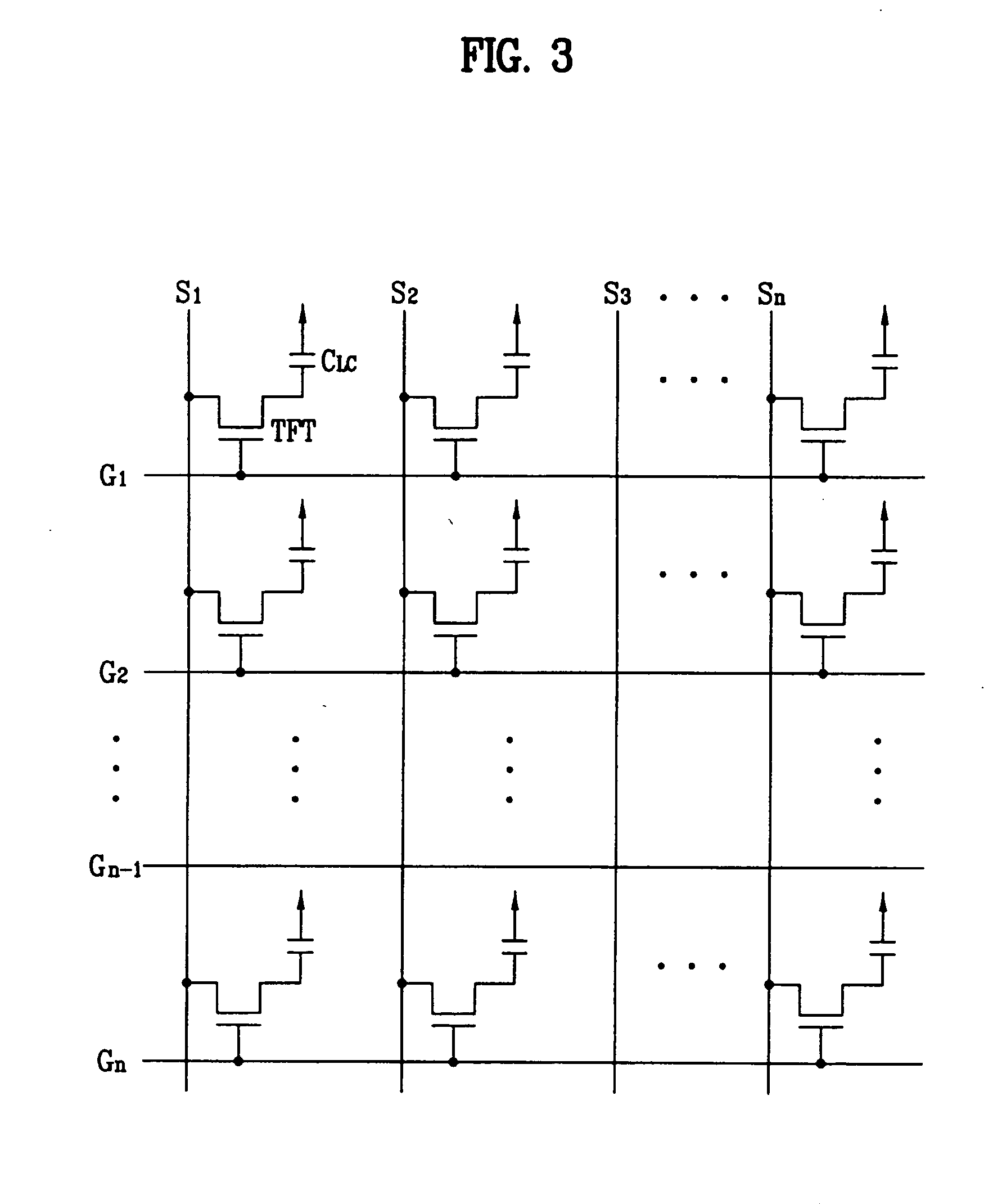
Liquid crystal display device
- Summary
- Abstract
- Description
- Claims
- Application Information
AI Technical Summary
Benefits of technology
Problems solved by technology
Method used
Image

Examples
first embodiment
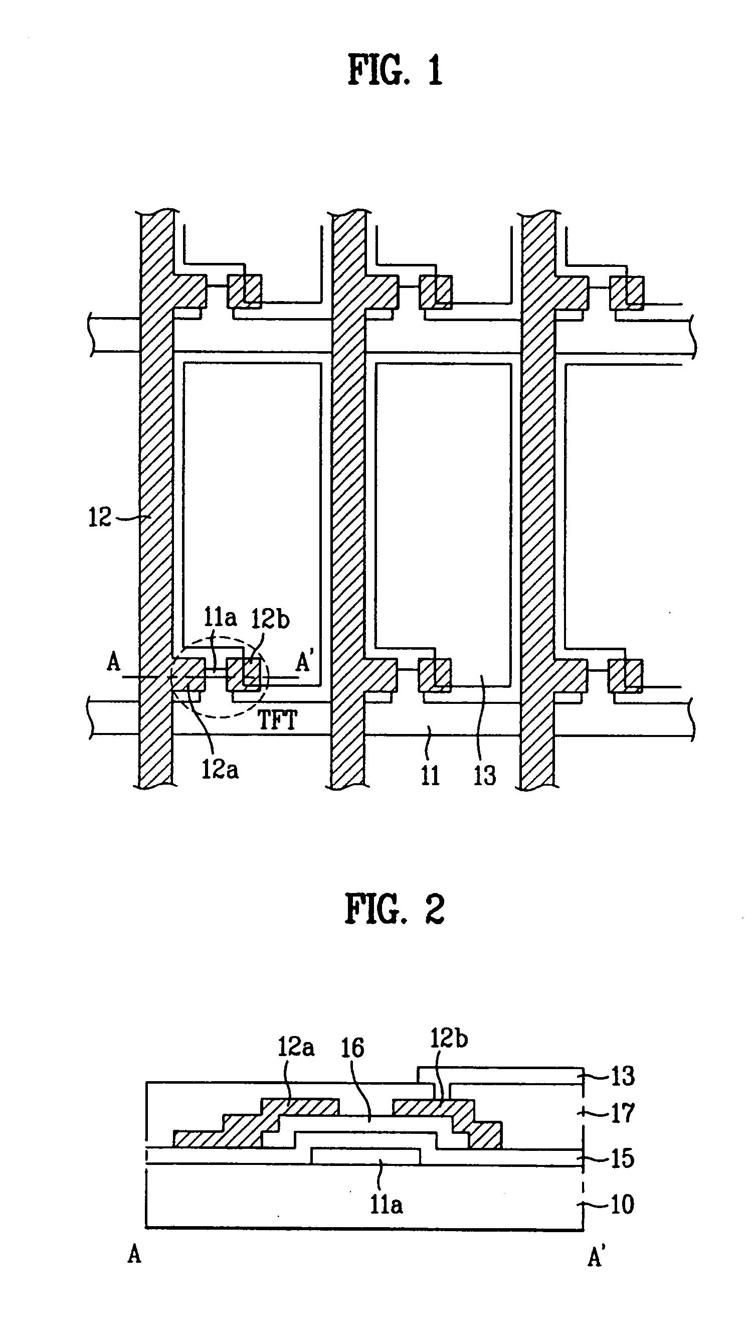
[0084]FIG. 4 is a plan view of an LCD device according to the present invention. As shown in FIG. 4, in the LCD device according to the present invention, data is provided in a time-divided manner to left and right side pixels of one data line. That is, the LCD device according to the embodiment shown includes a plurality of pairs of gate lines, each pair of gate lines including first and second gate lines 21 and 22 adjacent to each other, and a plurality of data lines 23 perpendicular to the respective gate lines 21 and 22, thereby defining the respective left and right side pixel regions. A right side pixel electrode 24a is formed in the right side pixel region and is driven by the first gate line 21. A left side pixel electrode 24b is formed in the left side pixel region and is driven by the second gate line 22.
[0085] The first and second gate lines 21 and 22 are perpendicular to the data lines, and first and second thin film transistors TFT1 and TFT2 respectively drive the right...
second embodiment
[0097] Referring to FIG. 8, a gate driver of an LCD device according to the present invention includes a gate drive IC 70 outputting a scanning signal GD1, GD2, . . . to each pair of gate lines, and switching parts T1 and T2 turned-on by first and second clock signals HC1 and HC2 applied from a system, for respectively applying signals G1, G2, G3, G4, . . . time-divided from the scanning signals GD1, GD2, . . . to the first and second gate lines of each pair.
[0098] The gate driver of the LCD device according to the second embodiment of the present invention includes the two switching parts T1 and T2 in each output terminal of the gate drive IC 70, so that it is possible to apply the gate signal G1, G2, G3, G4, . . . time-divided from the scanning signal GD1, GD2, . . . output from the gate drive IC 70. Unlike the LCD device according to the first embodiment of the present invention, in the LCD device according to the second embodiment of the present invention, it is possible to appl...
third embodiment
[0108] Even though there are twice as many gate lines of the LCD device as those in the LCD deice according to the related art, a selection block of the signal applied to each gate line is the half of that according to the related art, so that the LCD device spends the same time in scanning the first gate line to the last gate line at each frame as that according to the related art.
[0109]FIG. 11 is a truth table illustrating that a gate line is selectively driven according to a clock signal when driving a gate line of an LCD device according to the second and third embodiments of the present invention; and FIG. 12 is a timing view illustrating that an output of a gate driver is provided in a time-divided manner when applying one pair of gate lines of an LCD device according to the second and third embodiments of the present invention.
[0110] As shown in FIG. 11, in the gate driver according to the second and third embodiments of the present invention, the gate signal G1, G3, . . . ...
PUM
 Abstract
Description
Claims
Application Information