
Display panel and method of manufacturing the same

Active Publication Date: 2016-04-28
SAMSUNG DISPLAY CO LTD
View PDF4 Cites 2 Cited by
  • Summary
  • Abstract
  • Description
  • Claims
  • Application Information

AI Technical Summary

Benefits of technology

This patent is about a display panel that can make things more transparent. The invention uses a special design that increases the amount of light that passes through the panel. This makes things look brighter and clearer. The manufacturing process for the display panel is simplified because the design uses the same material as the gate pattern. This saves money on the manufacturing costs.

Problems solved by technology

However, the PVA mode has disadvantages, such as an afterimage and a poor side viewing angle.
The IPS mode also has disadvantages, such as low luminance.
Accordingly, it is difficult to form the gate electrode and the common electrode by the same material.
However, the plasmonic color filter requires an additional manufacturing process, so that a manufacturing cost may be increased.

Method used


Image

  • Display panel and method of manufacturing the same
  • Display panel and method of manufacturing the same
  • Display panel and method of manufacturing the same

Examples


Embodiment Construction

[0041]Hereinafter, embodiments will be explained in detail with reference to the accompanying drawings.

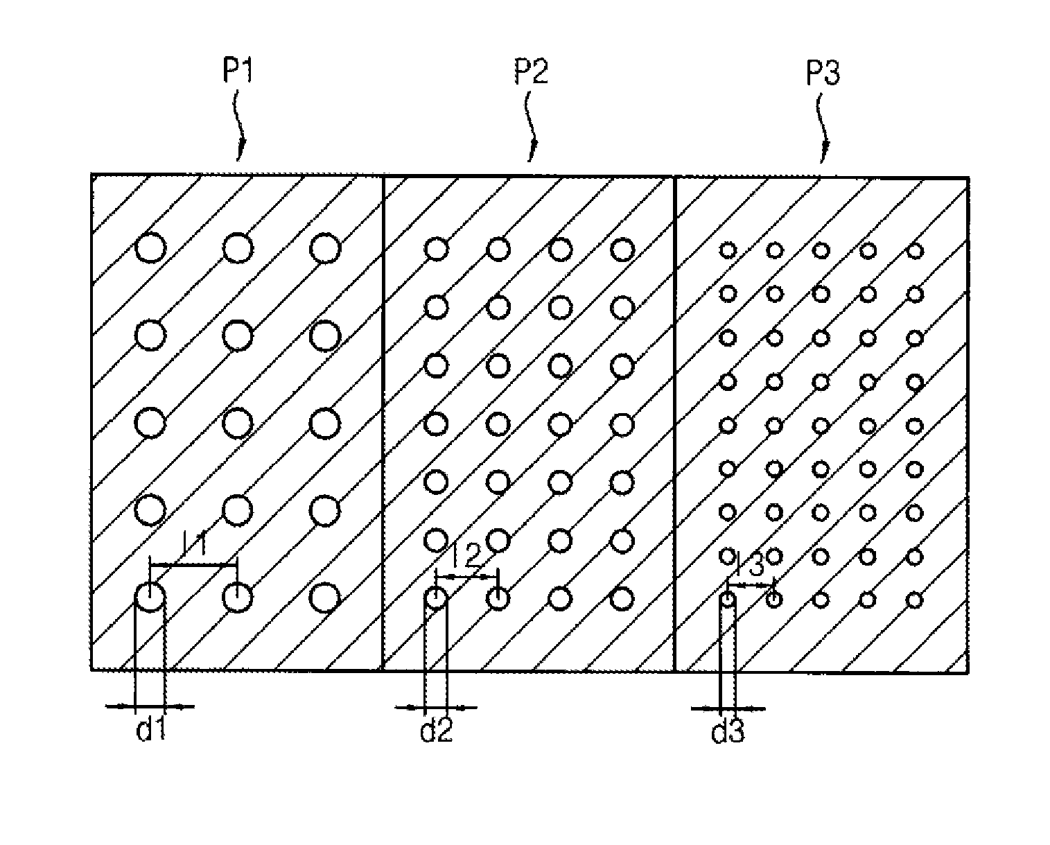
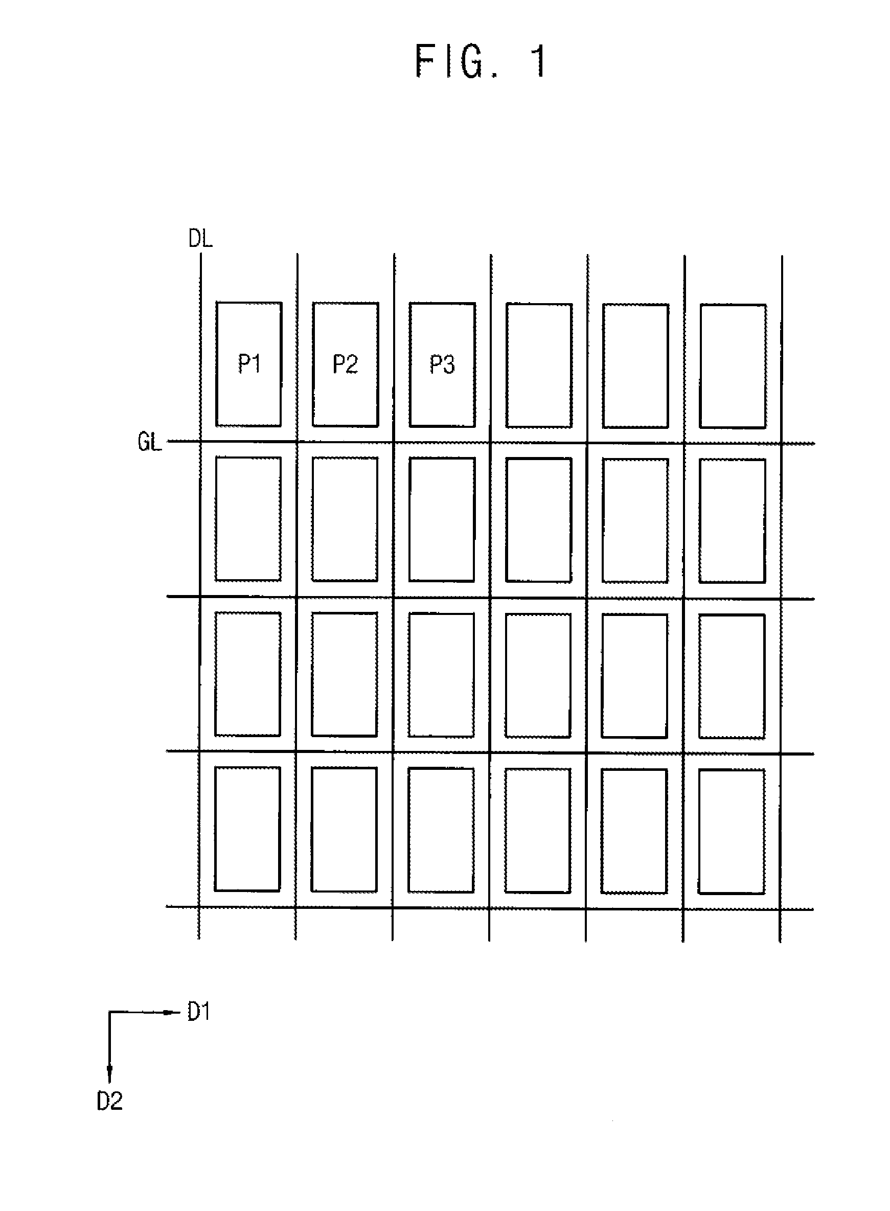
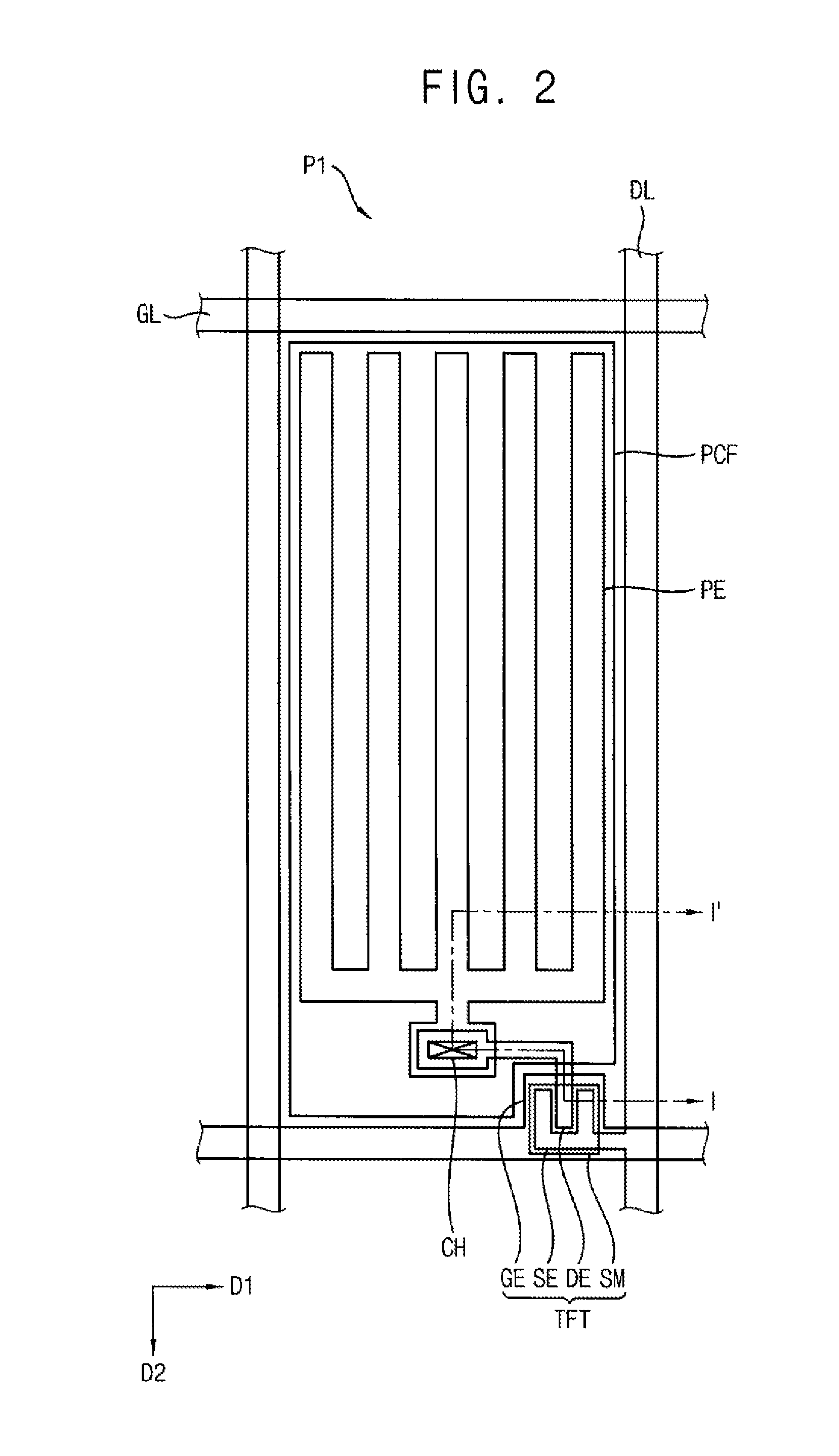
[0042]FIG. 1 is a plan view illustrating a display panel according to an exemplary embodiment of the present inventive concept. FIG. 2 is a plan view illustrating a first pixel of FIG. 1. FIG. 3 is a cross-sectional view taken along a line I-I′ of FIG. 2. FIG. 4 is a plan view illustrating plasmonic color filters of first to third pixels of FIG. 1. FIG. 5 is a cross-sectional view illustrating a plasmonic color filter according to an exemplary embodiment of the present inventive concept.

[0043]Referring to FIG. 1, a display panel according to an exemplary embodiment of the present inventive concept panel includes a plurality of gate lines GL, a plurality of data lines DL and a plurality of pixels.

[0044]The gate lines GL may extend in a first direction D1. The data lines DL may extend in a second direction D2 substantially perpendicular to the first direction D1. Alternatively, the g...


PUM


Abstract

A display panel includes a first substrate comprising a plurality of pixel areas, a second substrate facing the first substrate, a liquid crystal layer interposed between the first substrate and the second substrate, a thin film transistor comprising a gate electrode disposed on the first substrate, a semiconductor pattern overlapping with the gate electrode, a source electrode and a drain electrode overlapping with the semiconductor pattern and spaced apart from each other, a plasmonic color filter to which a common voltage is configured to be applied, and comprising a same material as the gate electrode, disposed on a same layer as the gate electrode, and comprising a plurality of holes through which light is configured to be transmitted and a pixel electrode to which a gray scale voltage is configured to be applied, and overlapping with the plasmonic color filter, and electrically connected to the drain electrode.

Description

CROSS-REFERENCE TO RELATED APPLICATIONS[0001]This application claims priority under 35 U.S.C. §119 to Korean Patent Application No. 10-2014-0146351, filed on Oct. 27, 2014 in the Korean Intellectual Property Office KIPO, the contents of which are herein incorporated by reference in their entireties.BACKGROUND[0002]1. Field[0003]Exemplary embodiments of the present inventive concept relate to a display panel and method of manufacturing the display panel.[0004]2. Description of the Related Art[0005]A liquid crystal display apparatus is one of a flat panel display FPD, which is used broadly recently. Examples of the flat panel display include, but are not limited to, a liquid crystal display (“LCD”), a plasma display panel (“PDP”) and an organic light emitting display (“OLED”).[0006]The liquid crystal display apparatus applies voltages to molecules of liquid crystal to adjust arrangements of the molecules thereby changing optical characteristics of a liquid crystal cell such as birefri...

Claims


Application Information

Patent Timeline
IPC IPC(8): G02F1/1335H01L27/12G02F1/1362G02F1/1341G02F1/1343G02F1/1368
CPCG02F1/133514G02F1/13439G02F1/1368G02F1/136286H01L27/1259G02F1/136209G02F1/1341H01L27/124G02F1/134309G02F2203/10G02F1/134372G02F1/136222
Inventor SON, JUNG-HALEE, JOO-HYUNGYEO, YUN-JONG
Owner SAMSUNG DISPLAY CO LTD
Learn More