Data synchronizing signal detecting device

a data synchronization and signal detection technology, applied in the field of signal processing devices, can solve the problems of reducing the detection error of sync signals, improving the data discrimination performance of a data discriminator, and requiring positive improvement of sync signal detection performan

Inactive Publication Date: 2005-03-10
HITACHI GLOBAL STORAGE TECH JAPAN LTD
View PDF18 Cites 0 Cited by
  • Summary
  • Abstract
  • Description
  • Claims
  • Application Information

AI Technical Summary

Benefits of technology

[0025] Accordingly, the present invention is required to reduce the detection error of sync signals. Also, an improved data discrimination performance of a data discriminator may be reflected in a deteriorated sync signal detection performance of a sync signal detector. In such a case, the sync signal detection performance is required to be positively improved with respect to the data discrimination performance.

Problems solved by technology

Also, an improved data discrimination performance of a data discriminator may be reflected in a deteriorated sync signal detection performance of a sync signal detector.

Method used


Image

  • Data synchronizing signal detecting device
  • Data synchronizing signal detecting device
  • Data synchronizing signal detecting device

Examples


first embodiment

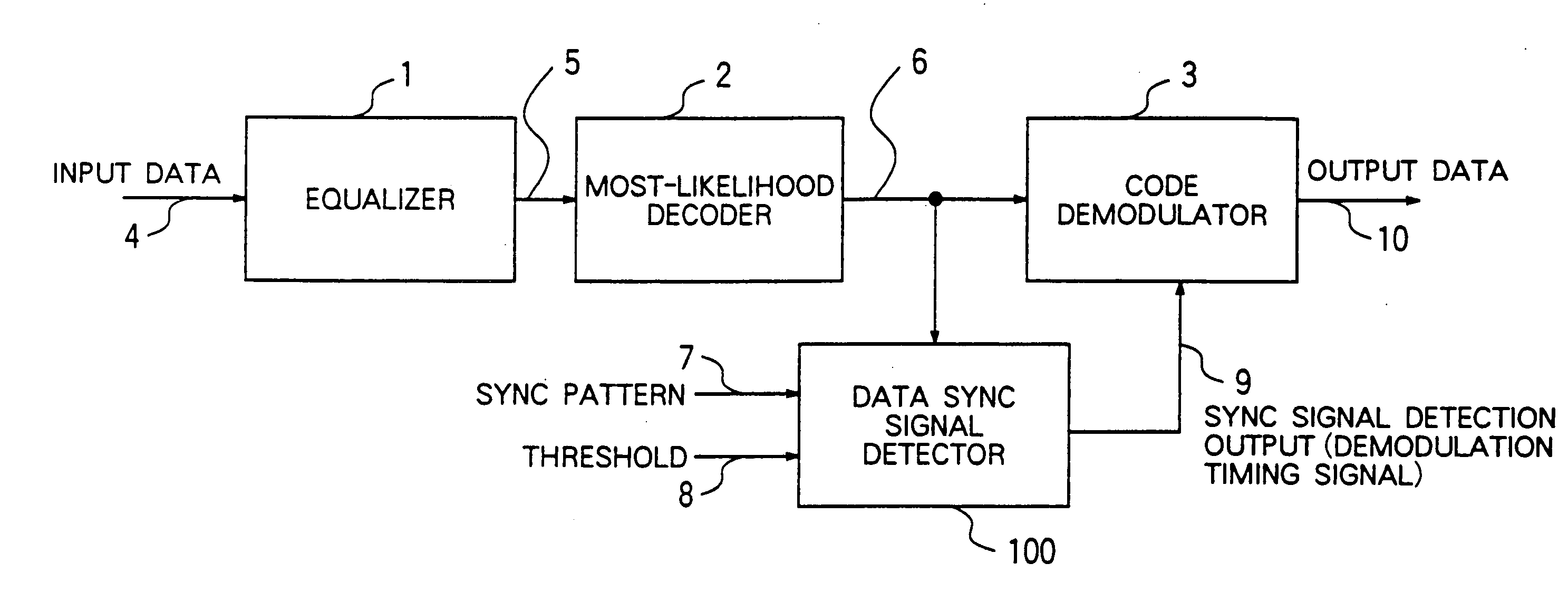
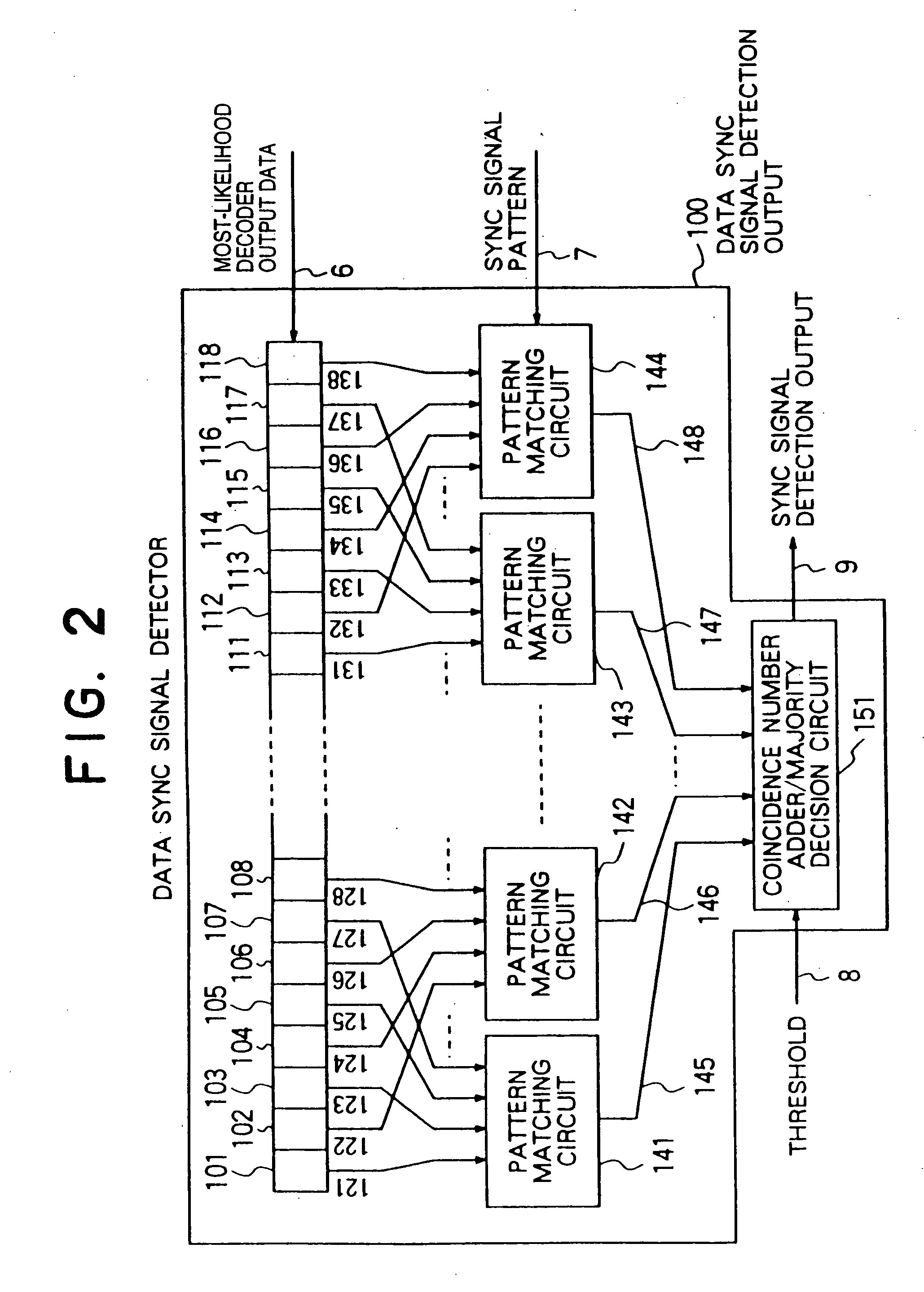
[0068] The configuration and operation of a data sync signal detector according to the invention will be described more specifically with reference to FIG. 3.

[0069] In the first embodiment, the total number of groups is 2, the threshold value is 1 and each group is configured of five bits, for example.

[0070] The output data 6 of the most-likelihood decoder is applied to the bit cell of the shift register 310 and sequentially shifted and held in the shift register bit cells 309 to 301.

[0071] The shift register bit cell outputs 321 to 330 are separated into an odd-numbered string and an even-numbered string input and applied to pattern matching circuits 341 and 342, respectively. In other words, the shift register bit cell outputs 321, 323, 325, 327, 329 of the odd-numbered string are applied to the pattern matching circuit 341, and the shift register bit cell outputs 322, 324, 326, 328, 330 of the even-numbered string are applied to the pattern matching circuit 342.

[0072] The odd-...

second embodiment

[0105] Now, the invention will be explained with reference to FIG. 4.

[0106] The second embodiment concerns an example in which the number of the groups is 2, the threshold value is 1 and each group is configured of 6 bits.

[0107] The output data 6 of the most-likelihood decoder is input to a shift register bit cell 412 and shifted and held in the bit cells 411 to 401 sequentially.

[0108] The shift register bit cell outputs 421 to 432 are separated into an odd-numbered string and an even-numbered string and input to pattern matching circuits 441 and 442. Specifically, the shift register bit cell outputs 421, 423, 425, 427, 429, 431 of the odd-numbered string are applied to the pattern matching circuit 441, and the shift register bit cell outputs 422, 424, 426, 428, 432 of the even-numbered string are input to the Pattern matching circuit 442.

[0109] The odd-numbered string is matched with “010011” as a predetermined sync pattern, and the result 443 thereof is output. The even-numbere...

third embodiment

[0122] Now, the invention will be explained with reference to FIG. 5.

[0123] This third embodiment concerns a case in which the total number of groups 4, the threshold hold value is 2 and each group is configured of four bits. The most-likelihood decoder output data 6 is applied to a shift register bit cell 516 and sequentially shifted and held in bit cells 515 to 501. Shift register bit cell outputs 521 to 536 are separated into odd-numbered strings and even-numbered strings and applied to pattern matching circuits 541 to 544.

[0124] Specifically, the shift register bit cell outputs 521, 523, 525, 527 of the first-half odd-numbered string are applied to the pattern matching circuit 541, and the shift register bit cell outputs 529, 531, 533, 535 of the last-half odd-numbered string are applied to the pattern matching circuit 543.

[0125] The shift register bit cell outputs 522, 524, 526, 528 of the first-half even-numbered string, on the other hand, are applied to the pattern matching...


PUM

PropertyMeasurementUnit
storage areaaaaaaaaaaa
recording densityaaaaaaaaaa
transmissionaaaaaaaaaa

Abstract

A data sync signal detecting device for detecting a sync signal having sync signal detection errors. The detecting device applies the output data of a most-likelihood decoder to shift register bit cells. The data is sequentially shifted and held in the bit cells of the shift register. The bit cell outputs are separated into odd-numbered and even-numbered bit string and applied to first and second pattern matching circuits. The odd-numbered bit string is matched with “01001”; by a first pattern matching circuit. The even-numbered bit string is matched with “01011” by a second pattern matching circuit. First and second matching results are applied to a coincidence number adder/majority decision circuit. When coincidence occurs, the matching result is “1”, and when non-coincidence occurs, the matching result is “0”. The coincidence number adder/majority decision circuit produces a sync signal detection output when the first or second matching result is “1”.

Description

[0001] The present application is a continuation of application Ser. No. 10 / 244,516, filed Sep. 17, 2002; which is a continuation of application Ser. No. 09 / 837,264, filed Apr. 19, 2001, now U.S. Pat. No. 6,473,477; which is a continuation of application Ser. No. 09 / 570,037, filed May 12, 2002, now U.S. Pat. No. 6,259,753; which is a continuation of application Ser. No. 08 / 948,942, filed Oct. 10, 1997, now U.S. Pat. No. 6,125,156, the contents of which are incorporated herein by reference.BACKGROUND OF THE INVENTION [0002] The present invention generally relates to a signal processing device, and in particular to a data synchronizing (sync) signal detecting device with an improved sync signal detection rate which can detect a sync signal even in the case where a sync signal section has a data discrimination error. [0003] An example of the conventional sync signal detecting device will be explained with reference to FIGS. 9 and 10. [0004] A magnetic disk device is referred to as an e...

Claims


Application Information

Patent Timeline
Patent Type & Authority Applications(United States)
IPC IPC(8): G11B20/10G11B20/12G11B20/14G11B20/18G11B27/30H04L7/04
CPCG11B20/1217H04L7/042G11B2220/20G11B27/3027
Inventor WATANABE, YOSHIJU
Owner HITACHI GLOBAL STORAGE TECH JAPAN LTD
Why Eureka
Try Eureka