Semiconductor structures employing strained material layers with defined impurity gradients and methods for fabricating same

a technology of impurity gradients and semiconductors, applied in the direction of semiconductor devices, electrical equipment, transistors, etc., can solve the problems of structure and device performance not showing the degraded effect, and achieve the effect of improving operational performan

Inactive Publication Date: 2005-03-10
TAIWAN SEMICON MFG CO LTD
View PDF99 Cites 17 Cited by
  • Summary
  • Abstract
  • Description
  • Claims
  • Application Information

AI Technical Summary

Benefits of technology

[0018] The present invention provides semiconductor structures and devices (e.g., FETs) that include one or more strained material layers that not only improve operational performance, but also are relatively f

Problems solved by technology

Consequently, the resulting semiconductor structures and devices do not exhibit the degra

Method used


Image

  • Semiconductor structures employing strained material layers with defined impurity gradients and methods for fabricating same
  • Semiconductor structures employing strained material layers with defined impurity gradients and methods for fabricating same
  • Semiconductor structures employing strained material layers with defined impurity gradients and methods for fabricating same

Examples


Embodiment Construction

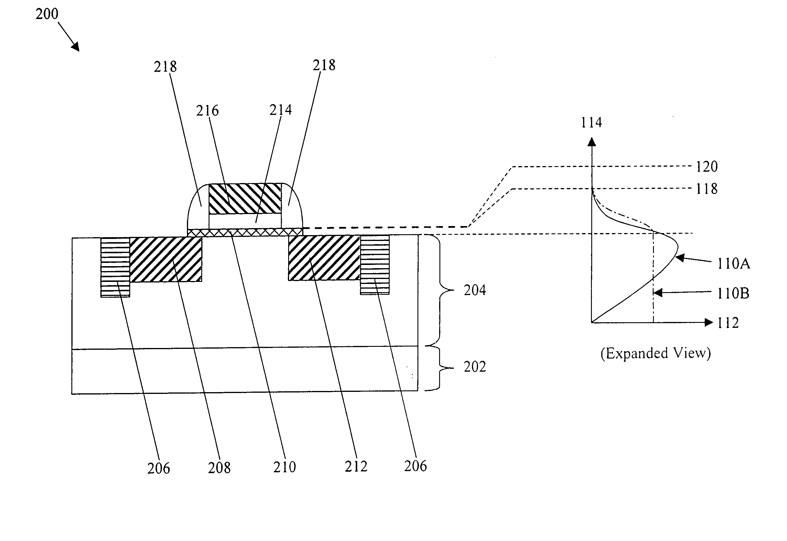
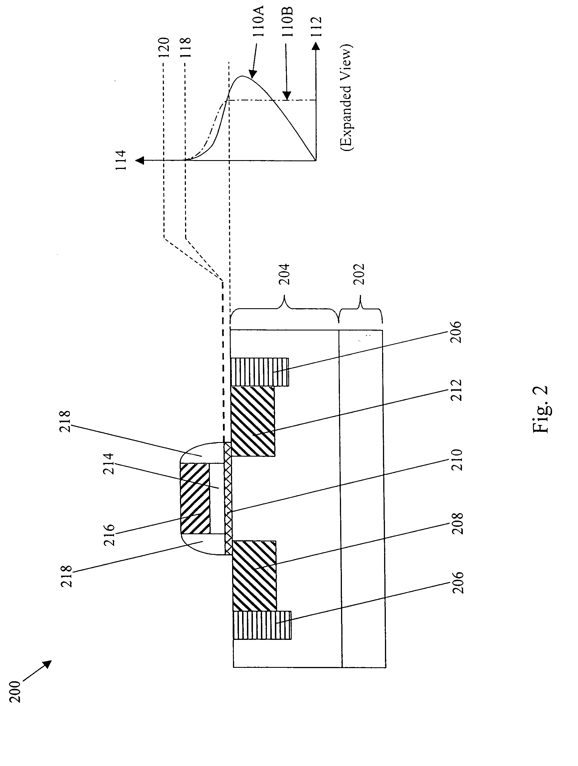
[0032] As shown in the drawings for the purposes of illustration, the invention may be embodied in a semiconductor structure or device, such as, for example, a FET, with specific structural features. A semiconductor structure or FET according to the invention includes one or more strained material layers that are relatively free of interdiffused impurities. These strained material layers are characterized by at least one diffusion impurity gradient that has a value that is substantially equal to zero in a particular area of the strained layer. Consequently, the semiconductor structure or FET does not exhibit the degraded performance that results from the presence of such impurities in certain parts of the strained layers.

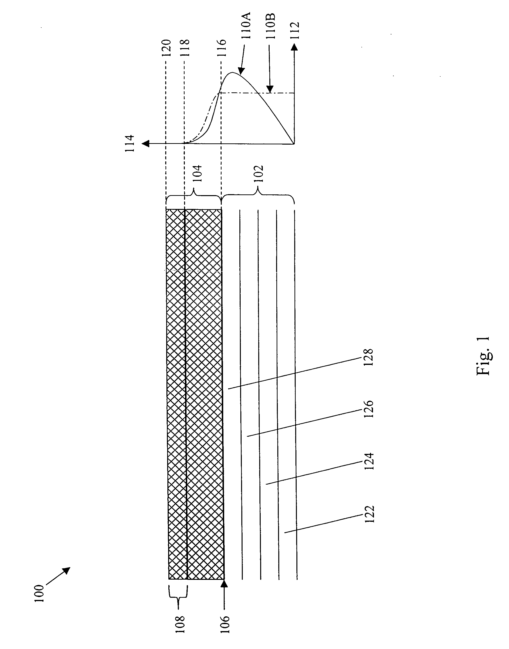
[0033] In brief overview, FIG. 1 depicts a schematic (unscaled) cross-sectional view of a semiconductor structure 100 in accordance with an embodiment of the invention. The semiconductor structure 100 includes a substrate 102. The substrate 102 may be Si, SiGe, or ...


PUM


Abstract

Semiconductor structures and devices including strained material layers having impurity-free zones, and methods for fabricating same. Certain regions of the strained material layers are kept free of impurities that can interdiffuse from adjacent portions of the semiconductor. When impurities are present in certain regions of the strained material layers, there is degradation in device performance. By employing semiconductor structures and devices (e.g., field effect transistors or “FETs”) that have the features described, or are fabricated in accordance with the steps described, device operation is enhanced.

Description

CROSS-REFERENCE TO RELATED APPLICATION [0001] This application claims priority to and the benefit of, and incorporates herein by reference, in its entirety, provisional U.S. patent application Ser. No. 60 / 324,325, filed 21 Sep. 2001.FIELD OF THE INVENTION [0002] The present invention relates generally to semiconductor structures and devices and, more specifically, to semiconductor structures and field effect transistors (hereinafter, “FETs”) incorporating strained material layers and controlled impurity diffusion gradients. BACKGROUND OF THE INVENTION [0003]“Virtual substrates” based on silicon (Si) and germanium (Ge) provide a platform for new generations of VLSI devices that exhibit enhanced performance when compared to devices fabricated on bulk Si substrates. The important component of a SiGe virtual substrate is a layer of SiGe that has been relaxed to its equilibrium lattice constant (i.e., one that is larger than that of Si). This relaxed SiGe layer can be directly applied to...

Claims


Application Information

Patent Timeline
IPC IPC(8): H01L21/20H01L21/02H01L21/338H01L27/12H01L29/10H01L29/36H01L29/778H01L29/78H01L29/786H01L29/812
CPCH01L29/105H01L29/1054H01L29/36H01L29/66477H01L29/66651H01L29/78Y10S438/926H01L29/66545H01L29/161H01L29/7842
Inventor CURRIE, MATTHEWLOCHTEFELD, ANTHONYHAMMOND, RICHARDFITZGERALD, EUGENE
Owner TAIWAN SEMICON MFG CO LTD
Why Eureka
Try Eureka