Plasma display panel driver and plasma display device

Inactive Publication Date: 2005-03-17
SAMSUNG SDI CO LTD
View PDF6 Cites 19 Cited by
  • Summary
  • Abstract
  • Description
  • Claims
  • Application Information

AI Technical Summary

Benefits of technology

[0028] It may be an advantage of the present invention to provide an improved PDP driving circuit for minimizing the impedance provided on a main discharge path.
[0029] It may be another advantage of the present invention to provide a PDP driving circuit for minimizing pattern impedance by allowing no switches on the path provided between a sustain discharge circuit and a panel electrode.
[0030] In one aspect of the present invention, a driver for a PDP including discharge cells with a plurality of electrodes, comprises: a first voltage source having a first voltage level; a first active element for intercepting a current flow in the direction of the first voltage source; a first switch coupled between the first active element and an electrode; a capacitor for storing a second voltage; and a second switch for supplying the second voltage stored in the capacitor to the electrode.
[0031] The first active element and the first switch may be realized by a first transistor and a second transistor respectively, and the first and second transistors may be coupled with each other in a back-to-back manner.
[0032] A source of the first transistor may be coupled to the first voltage source, and drains of the first and second transistors may be coupled with each other in a back-to-back manner.
[0033] The drain of the first transistor may be coupled to the first voltage source, and sources of the first and second transistors may be coupled with each other in a back-to-back manner.

Problems solved by technology

Therefore they problematically require resistors for current restriction.
Thus, they have a longer lifespan than DC plasma displays.
However, the switches Ypp and Ynp formed on the main discharge path are causes to increase pattern impedance.

Method used


Image

  • Plasma display panel driver and plasma display device
  • Plasma display panel driver and plasma display device
  • Plasma display panel driver and plasma display device

Examples


first embodiment

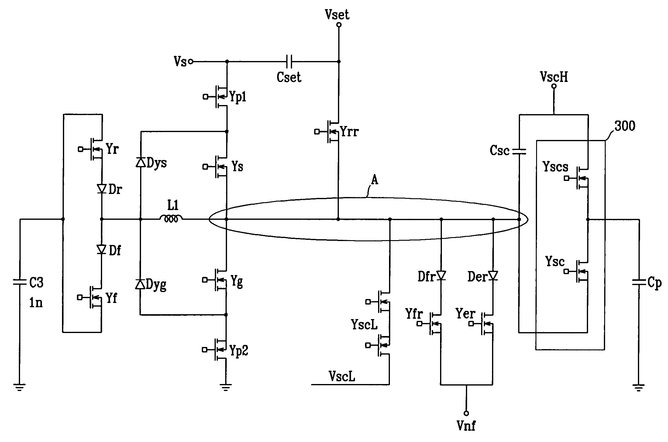
[0056] Further, the first embodiment comprises a scan driver including voltage sources VscH and VscL, switches Yscs, Ysc, and YscL, and a capacitor Csc; a falling ramp driver including a diode Dfr and a transistor Yfr; and an erase driver including a diode Der and a transistor Yer. A constant current driver for allowing a driving waveform to ramp-fall can be coupled to gates of the transistors Yfr and Yer, though not illustrated. The scan driver, the falling ramp driver, and the erase driver can be realized by conventional circuits which perform the same operations, and the operations realized in the exemplary embodiment will be described later.

[0057] As known from FIG. 7, no switches may be provided on the main discharge path A provided between the sustain discharge circuit and the electrode, and hence, no pattern impedance according to the main discharge path may be generated in a like manner of the prior art.

[0058]FIG. 8 shows a timing diagram of a driving waveform of a scan ele...

second embodiment

[0071] The second embodiment may perform the sustain discharge, erase, reset, and address operations according to the timing diagram shown in FIG. 8. Hence, no additional detailed descriptions on the operations is necessary.

[0072] However, the switch Yp3 may be arranged between the power recovery circuit and the electrode to reduce the withstanding voltage of the power recovery circuit during rising ramp operation in the reset period in the second embodiment.

[0073]FIGS. 12a and 12b show equivalent circuits of the first and second exemplary embodiments of the present invention in the case of ramp rising.

[0074] As shown in FIG. 12a, in the first embodiment, the voltage of (Vs+Vset) may be applied to the power recovery circuit. The switches Yp1, Yp2, Ys, and Yg may be turned off in the case of ramp rising, but the voltage of (Vs+Vset) may be applied to the power recovery circuit depicted by a circle by a body diode which occurs at the back-to-back coupling shown in FIGS. 5a and 5b. T...


PUM


Abstract

Disclosed is a driver for a PDP including discharge cells with a plurality of electrodes, which may include the following: a first voltage source having a first voltage level; a first active element for intercepting a current flow in the direction of the first voltage source; a first switch coupled between the first active element and an electrode; a capacitor for storing a second voltage; and a second switch for supplying the second voltage stored in the capacitor to the electrode. The first active element and the first switch may each be transistors, and they may be coupled together, back-to-back.

Description

CROSS REFERENCE TO RELATED APPLICATION [0001] This application claims priority to and the benefit of Korea Patent Application No. 2003-58736 filed on Aug. 25, 2003, in the Korean Intellectual Property Office, the entirety of which is incorporated herein by reference. BACKGROUND OF THE INVENTION [0002] 1. Field of the Invention [0003] The present invention relates to a plasma display panel (PDP) driving circuit. More specifically, the present invention relates to a driving circuit for preventing waveform distortion caused by impedance provided on a main discharge path. [0004] 2. Description of the Related Art [0005] Recently, liquid crystal displays (LCDs), field emission displays (FEDs), and plasma displays have been actively developed. The plasma displays panels (PDPs) from among the flat panel devices may have better luminance and light emission efficiency compared to the other types of flat panel devices, and also may have wider view angles. Therefore, the plasma displays may be ...

Claims


Application Information

Patent Timeline
IPC IPC(8): G09F9/313G09G3/20G09G3/288G09G3/291G09G3/296G09G3/298H01J17/49
CPCG09G2320/0223G09G3/2965G09G3/296
Inventor LEE, JUN-YOUNGJUNG, NAM-SUNGLEE, DONG-YOUNGAN, BYUNG-NAM
Owner SAMSUNG SDI CO LTD
Why Eureka
Try Eureka