Capacitorless 1-transistor DRAM cell and fabrication method

a technology of dram cell and capacitor, which is applied in the direction of transistors, electrical apparatus, semiconductor devices, etc., can solve the problems of necessary compromise and use of a comparatively expensive soi substra

Inactive Publication Date: 2005-03-24
POLARIS INNOVATIONS
View PDF5 Cites 163 Cited by
  • Summary
  • Abstract
  • Description
  • Claims
  • Application Information

AI Technical Summary

Benefits of technology

[0005] In one aspect, the present invention specifies a space-saving 1-transistor DRAM cell tha

Problems solved by technology

Disadvantages of this embodiment are the use of a comparatively expensive SOI substrate and the necessary

Method used


Image

  • Capacitorless 1-transistor DRAM cell and fabrication method
  • Capacitorless 1-transistor DRAM cell and fabrication method
  • Capacitorless 1-transistor DRAM cell and fabrication method

Examples


Embodiment Construction

[0013] The making and using of the presently preferred embodiments are discussed in detail below. It should be appreciated, however, that the present invention provides many applicable inventive concepts that can be embodied in a wide variety of specific contexts. The specific embodiments discussed are merely illustrative of specific ways to make and use the invention, and do not limit the scope of the invention.

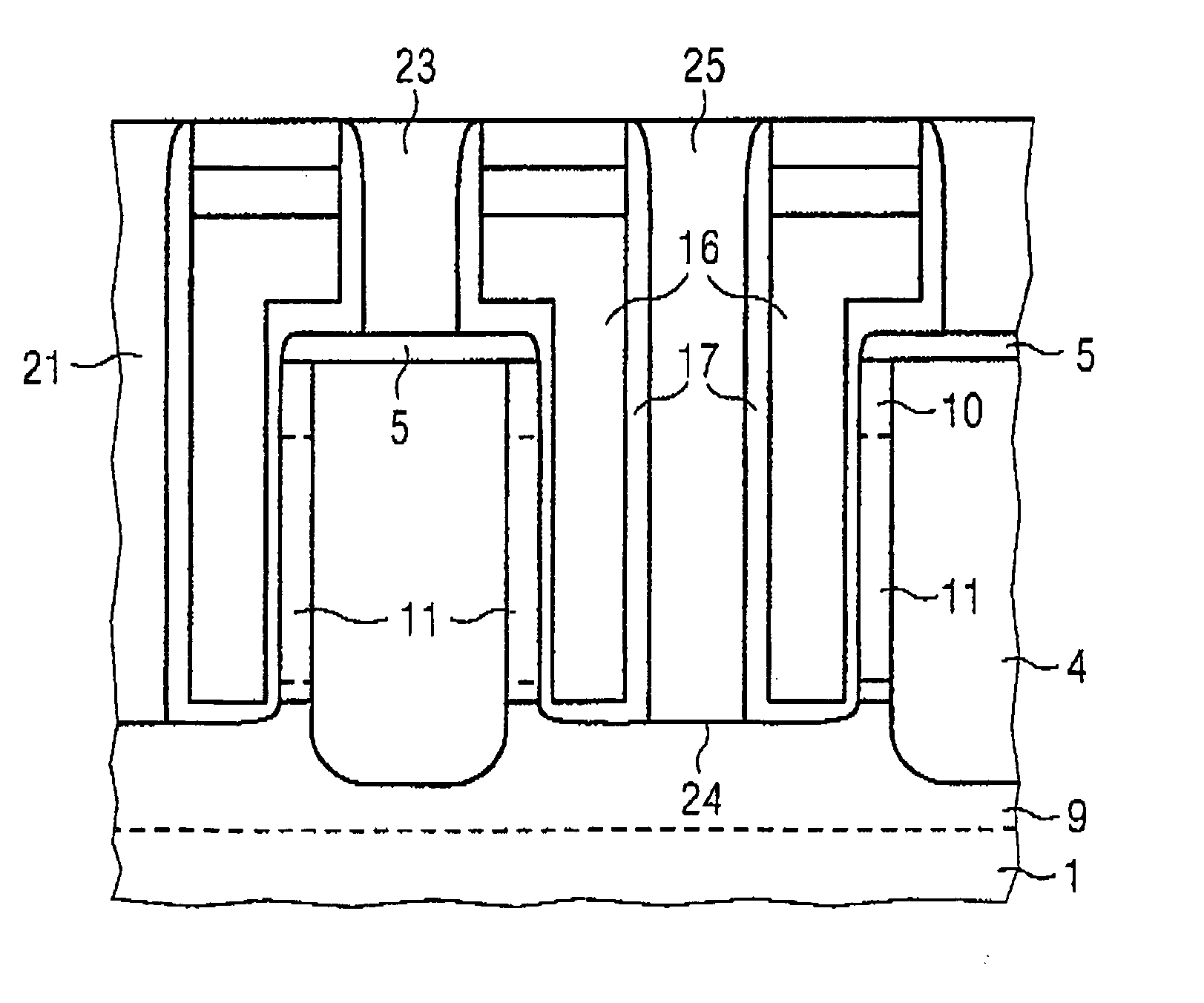
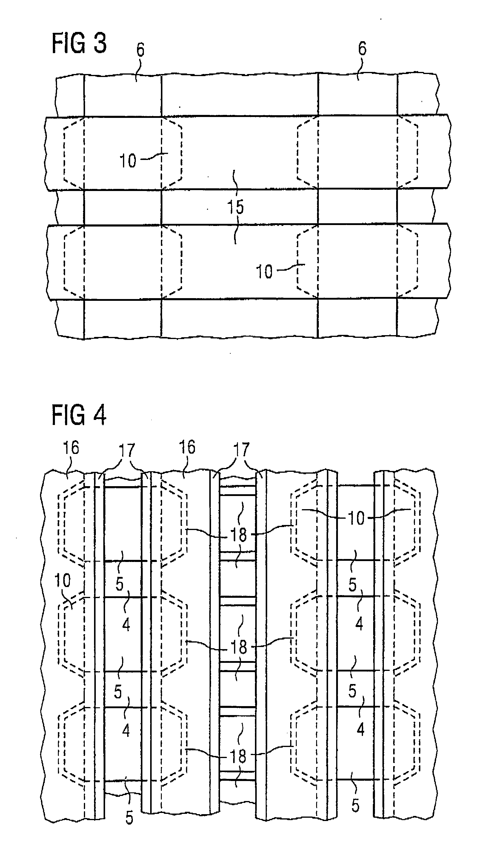
[0014] The orientation of the word lines WLj−1, WLj, WLj+1, and of the bit lines BLi, BLi+1, which are routed such that they run transversely above the word lines, is illustrated in a diagrammatic plan view of a memory cell array in FIG. 9. Broken lines additionally depict the positions of two cross-sections A and B; these positions correspond to the positions of the cross-sections of FIGS. 5 and 6, which will be explained below. A crosspoint DRAM architecture in accordance with the illustration of FIG. 9 manages with an area requirement of 4F2 per cell.

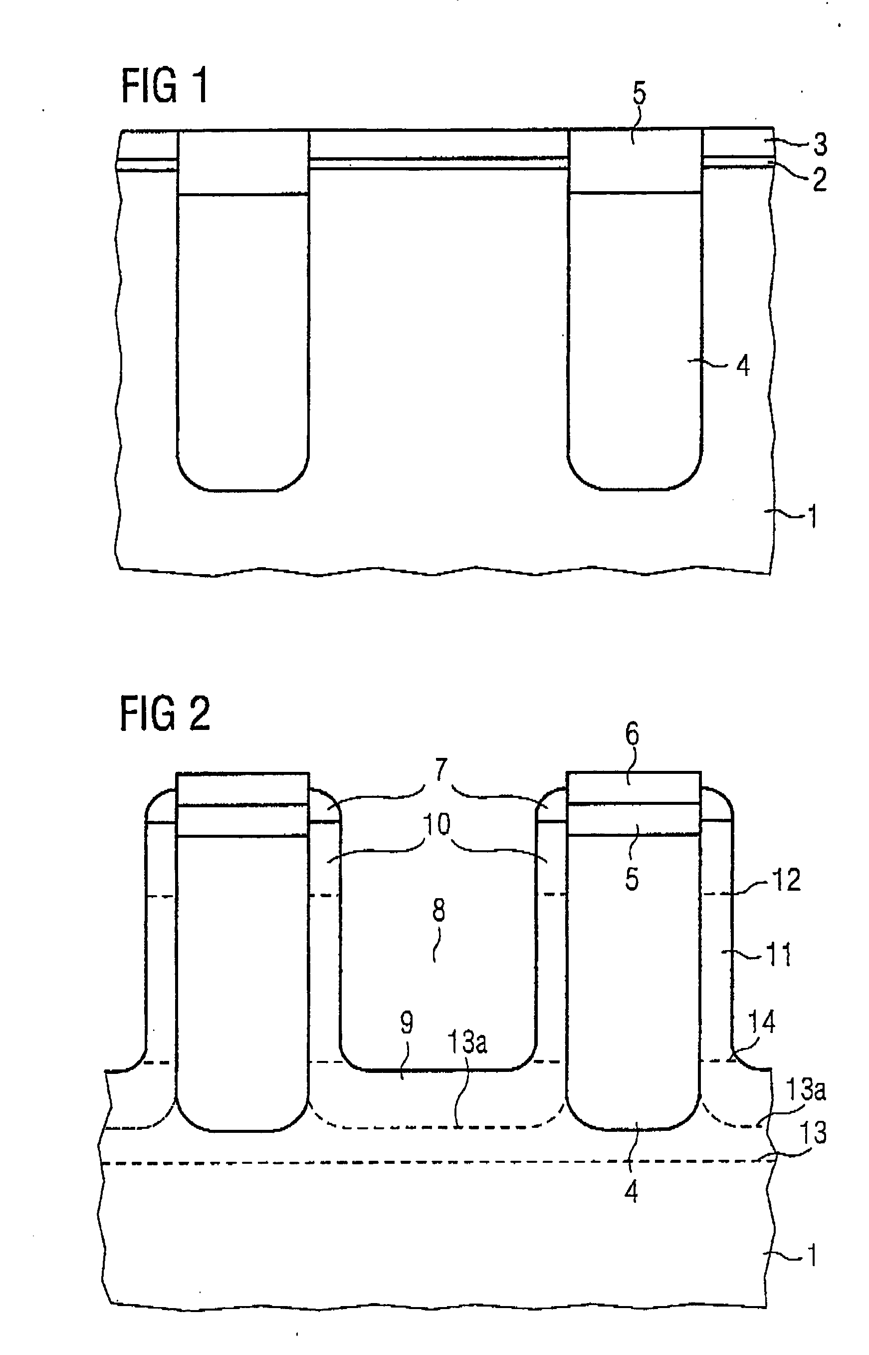
[0015] The structur...


PUM


Abstract

The channel region (11) and the source-drain regions (9, 10) are arranged vertically at a sidewall of a dielectric trench filling (4). On the opposite side, the semiconductor material is bounded by the gate dielectric (18) and the gate electrode (16), which is arranged in a cutout of the semiconductor material. A memory cell array comprises a multiplicity of vertically oriented strip-type semiconductor regions in which source-drain regions are implanted at the top and bottom and a channel region embedded in insulating material on all sides is present in between as a floating body.

Description

[0001] This application is a continuation of PCT application PCT / DE03 / 00181, filed on Jan. 23, 2003 and published in German on Aug. 14, 2003, which application claims priority to German patent application 102 04 871.1, filed Feb. 6, 2002. Both of these applications are incorporated herein by reference.TECHNICAL FIELD [0002] The present invention relates to a capacitorless 1-transistor DRAM cell, simply referred to as 1-transistor DRAM cell hereinafter, and an associated fabrication method. BACKGROUND [0003] S. Okhonin, M. Nagoga, J. M. Sallese and P. Fazan from the Ecole Polytechnique Fédérale de Lausanne (Preprint and Presentation at the IEEE SOI Conference, ISS / EPFL 2001) have proposed an embodiment of DRAM cells in the sub-100 nm range in which the memory cell is arranged as transistor structure in the body silicon layer of an SOI substrate. This concept dispenses with a formation of a capacitor that is specially provided for each cell. The semiconductor material which comprises ...

Claims


Application Information

Patent Timeline
IPC IPC(8): H01L21/8242H01L27/108H01L27/12
CPCH01L27/108H01L27/10876Y10S257/906H01L29/7841H01L27/1203H10B12/00H10B12/053
Inventor WILLER, JOSEF
Owner POLARIS INNOVATIONS
Why Eureka
Try Eureka