Phase-change memory device and method that maintains the resistance of a phase-change material in a reset state within a constant resistance range

a phase-change memory and resistance technology, applied in semiconductor devices, digital storage, instruments, etc., can solve the problems of delay in the transition to the reset state, failure of the read operation, and non-uniform widths of the bottom contacts that contact the phase-change materials, so as to increase the complementary write current

Active Publication Date: 2005-03-31
SAMSUNG ELECTRONICS CO LTD
View PDF4 Cites 45 Cited by
  • Summary
  • Abstract
  • Description
  • Claims
  • Application Information

AI Technical Summary

Benefits of technology

[0022] The data provided to the phase-change memory cell is reset data. The write driver stores the data in the phase-change memory cell in response to the data and a reset pulse, receives the first through nth current control signals that are at the first level, increases an amount of the complementary write current, and provides the increased complementary write current to the phase-change memory cell.
[0023] The write driver comprises a first current control unit and a second current control unit. The first current control unit maintains a voltage level at a first node at the first level in response to a bias voltage, alters the voltage level at the first node to the second level in response to the data and the reset pulse, and provides the data to the phase-change memory cell. The second current control unit is turned off if the voltage level at the first node is at the first level, increases the complementary write current in response to the reset pulse and the first through nth current control signals that are at the first level, and outputs the increased complementary write current.
[0024] According to still another aspect of the present invention, there is provided a method of maintaining a resistance of a phase-change material in a reset state within a constant resistance range, the method comprises: providing reset data to a first phase-change memory cell; sensing data stored in the first phase-change memory cell; determining whether the sensed data and the data provided to the first phase-change memory cell are identical; providing a complementary write current to the first phase-change memory cell until the sensed data and the data provided to the first phase-change memory cell are identical; and providing the reset data to a second phase-change memory cell if the sensed data and the data provided to the first phase-change memory cell are identical. The complementary write current is increased when it is provided to the first phase-change memory cell.
[0025] According to yet another aspect of the present invention, there is provided a write driver including a first current control unit and a second current control unit. The first current control unit provides data to a phase-change memory cell in response to the data and a reset pulse. The second current control unit provides a complementary write current to the phase-change memory cell in response to first through nth current control signals if data stored in the phase-change memory cell and the data provided to the phase-change memory cell are not identical.
[0026] The first current control unit maintains a voltage level at a first node at a first level in response to a bias voltage, alters the voltage level at the first node to a second level in response to the data and the reset pulse, and provides the data to the phase-change memory cell.
[0027] The first through nth current control signals are generated at the first level if the data provided to the phase-change memory cell and the data stored in the phase-change memory cell are not identical, and the first through nth current control signals are generated at the second level if the data provided to the phase-change memory cell and the data stored in the phase-change memory cell are identical.

Problems solved by technology

Due to various reasons, however, such as defects arising during manufacturing, the widths of the bottom contacts that contact the phase-change materials may be non-uniform depending on the positions of the memory cells of a phase-change memory cell array.
In addition, in memory cells having non-uniform bottom contact widths, phase-change materials do not completely enter the reset state.
Thus, during the read operation, the resistances of the phase-change materials in the reset state may be non-uniform, causing failures during the read operation.
As a result, a transition to the reset state is delayed.
However, during an operation of reading data from the unit cell C, the normal sensing operation cannot be performed and sensing failures may occur during the read operation.
As such, due to manufacturing defects, the widths of bottom contacts that contact phase-change materials may vary among different unit cells in a phase-change memory cell array.
Thus, the phase-change materials of the unit cells in a reset state have different resistances and failures may occur during read operations.

Method used


Image

  • Phase-change memory device and method that maintains the resistance of a phase-change material in a reset state within a constant resistance range
  • Phase-change memory device and method that maintains the resistance of a phase-change material in a reset state within a constant resistance range
  • Phase-change memory device and method that maintains the resistance of a phase-change material in a reset state within a constant resistance range

Examples


Embodiment Construction

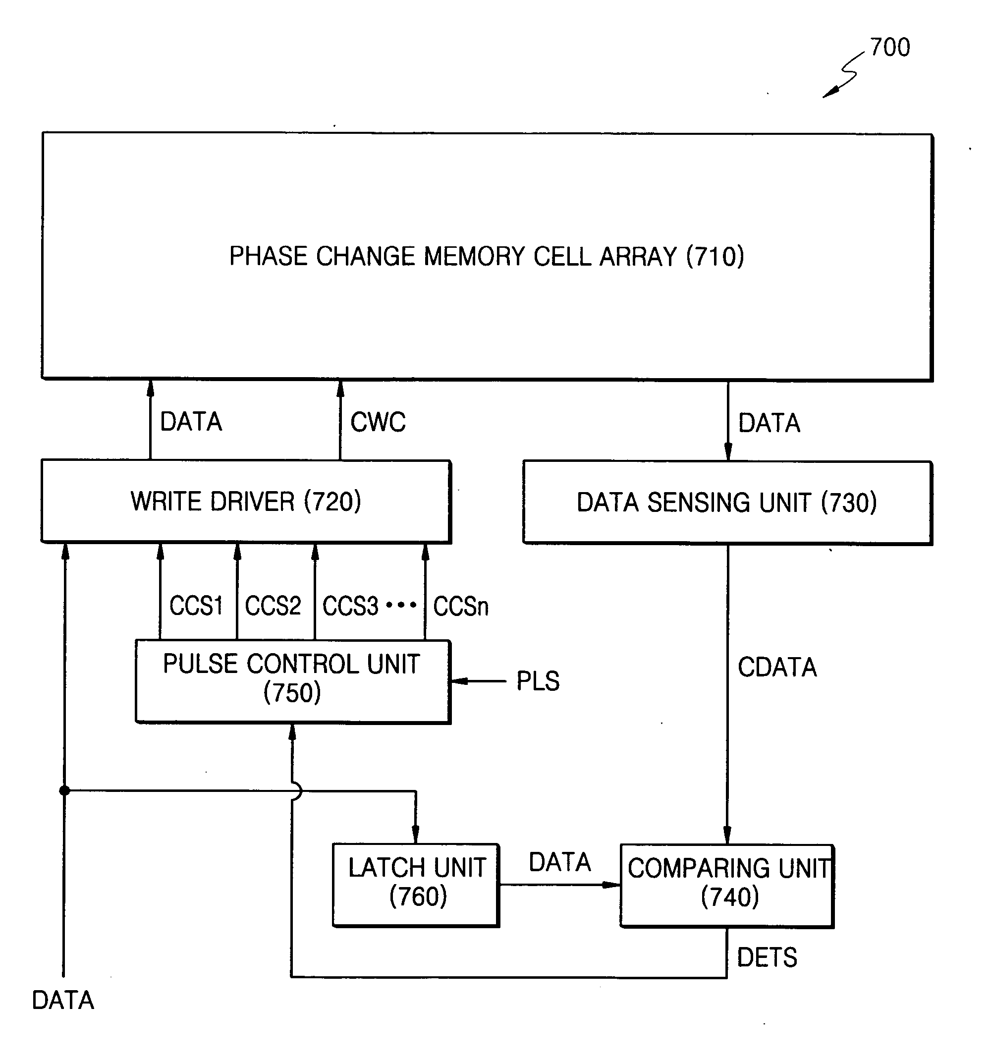
[0040]FIG. 4 is a flowchart illustrating a method 400 of maintaining a resistance of a phase-change material in a reset state within a constant resistance range, according to an exemplary embodiment of the present invention.

[0041] According to the method 400, reset data for causing a phase-change material of a phase-change memory cell to enter a reset state is provided to the phase-change memory cell, and then it is determined whether the phase-change memory cell has entered the reset state. During this time, current is provided to the phase-change material until the phase-change material has gone into the reset state. If it is determined that the phase-change material has gone into the reset state, reset data is provided to another phase-change memory cell.

[0042] As shown in FIG. 4, in step 410, data is provided to a phase-change memory cell. Here, the data is reset data. Step 410 is performed to enable the phase-change memory cell to stabilize in the reset state irrespective of ...


PUM


Abstract

Provided are a phase-change memory device and method that maintains a resistance of a phase-change material in a reset state within a constant resistance range. In the method, data is provided to a first phase-change memory cell and then it is first determined whether data stored in the first phase-change memory cell and the data provided to the first phase-change memory cell are identical. If the data stored in the first phase-change memory cell and the data provided to the first phase-change memory cell are not identical, a complementary write current is provided to the first phase-change memory cell and it is second determined whether the data stored in the first phase-change memory cell and the data provided to the first phase-change memory cell are identical. If the data stored in the first phase-change memory cell and the data provided to the first phase-change memory cell are identical, data is provided to a second phase-change memory cell.

Description

CROSS-REFERENCE TO RELATED APPLICATION [0001] This application claims priority to Korean Patent Application No. 2003-66504, filed on Sep. 25, 2003, in the Korean Intellectual Property Office, the disclosure of which is incorporated herein in its entirety by reference. BACKGROUND OF THE INVENTION [0002] 1. Technical Field [0003] The present invention relates to a phase-change memory device, and more particularly, to a phase-change memory device and method that maintains the resistance of a phase-change material used in the memory device within a constant resistance range in a reset state. [0004] 2. Discussion of the Related Art [0005] Phase-change random access memories (PRAMs) are non-volatile memory devices that store data using a phase-change material, e.g., Ge—Sb—Te (GST), whose resistance changes upon a phase transition due to a change in temperature. [0006] The phase-change material of a PRAM cell goes into a crystalline state or an amorphous state depending on the temperature ...

Claims


Application Information

Patent Timeline
Patent Type & Authority Applications(United States)
IPC IPC(8): G11C13/00G11C13/02G11C16/02G11C16/34H01L27/105H01L45/00
CPCG11C13/0004G11C13/0069G11C13/0064G11C13/02
Inventor CHOI, BYUNG-GILCHO, WOO-YEONGOH, HYUNG-ROKCHO, BEAK-HYUNG
Owner SAMSUNG ELECTRONICS CO LTD
Why Eureka
Try Eureka