

Plasma processing system
a processing system and semiconductor technology, applied in the direction of coatings, molten spray coatings, electric discharge tubes, etc., can solve the problems of large matching network types, high cost,
- Summary
- Abstract
- Description
- Claims
- Application Information
AI Technical Summary
Benefits of technology
Problems solved by technology
Method used
Image

Examples
Embodiment Construction
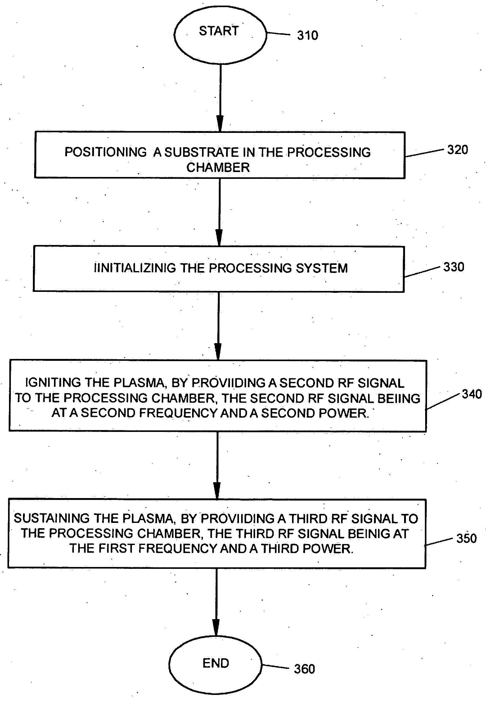
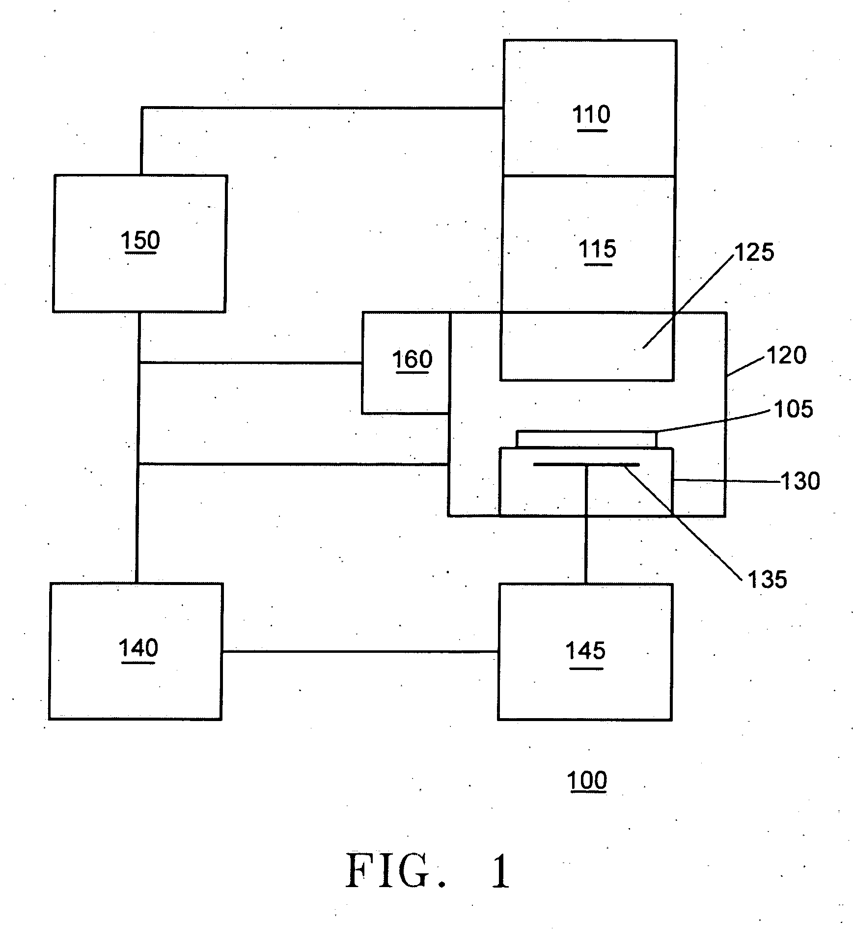
[0018] Referring now to the drawings, wherein like reference numerals designate identical, or corresponding parts throughout the several views, and more particularly to FIG. 1 thereof, FIG. 1 is an exemplary block diagram of a processing system in accordance with one embodiment of the present invention. The processing system 100 depicted in FIG. 1 can include an etch system, such as a plasma etcher. Alternately, the processing system 100 depicted in FIG. 1 can include a deposition system such as a chemical vapor deposition (CVD) system, a physical vapor deposition (PVD) system, an atomic layer deposition (ALD) system, and / or combinations thereof.
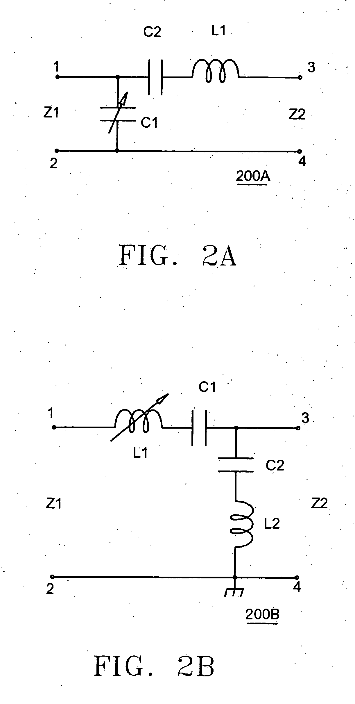
[0019] In one embodiment of the present invention, the processing system 100 includes a first RF source 110, a first matching network 115, processing chamber 120, monitoring system 160, and includes a second RF source 140, a second matching network 145, and controller 150. In addition, the processing chamber 120 can include a first electrod...
PUM
| Property | Measurement | Unit |
|---|---|---|
| Length | aaaaa | aaaaa |
| Fraction | aaaaa | aaaaa |
| Fraction | aaaaa | aaaaa |
Abstract
Description
Claims
Application Information