Optical system with particular optical distortion

a technology of optical distortion and optical system, which is applied in the field of optical system with particular optical distortion, can solve the problems of difficult to achieve nearly ideal performance, difficult to adequately correct all aberrations over the entire field of view, and viewed on a monitor screen is also subject to tv distortion, etc., and achieves hardly noticeable distortion of an actual image, high optical performance, and compact

Active Publication Date: 2005-04-07
FUJI PHOTO OPTICAL CO LTD
View PDF0 Cites 2 Cited by
  • Summary
  • Abstract
  • Description
  • Claims
  • Application Information

AI Technical Summary

Benefits of technology

The present invention relates to an optical system that can be extremely compact, uses a small number of lens components and lens elements, and can achieve high optical performance with hardly noticeable dist

Problems solved by technology

However, as the number of lens components and lens elements is reduced, it becomes more difficult to achieve nearly ideal performance.
However, with a very small number of lens components and/or lens elements, such as only two or three, it is difficult to adequately correct all of the aberrations over the entire field of view.
However, a picture viewed on a monitor screen is also subject to TV distortion independent of the optical distortion of

Method used


Image

  • Optical system with particular optical distortion
  • Optical system with particular optical distortion
  • Optical system with particular optical distortion

Examples


embodiments 1 and 2

of the present invention will now be individually described with further reference to the drawings. In the following descriptions, references will be frequently made to a “lens element.” However, as set forth above, it is understood that lens elements described below are also lens components and may variously be replaced by lens components that include more than one lens element.

embodiment 1

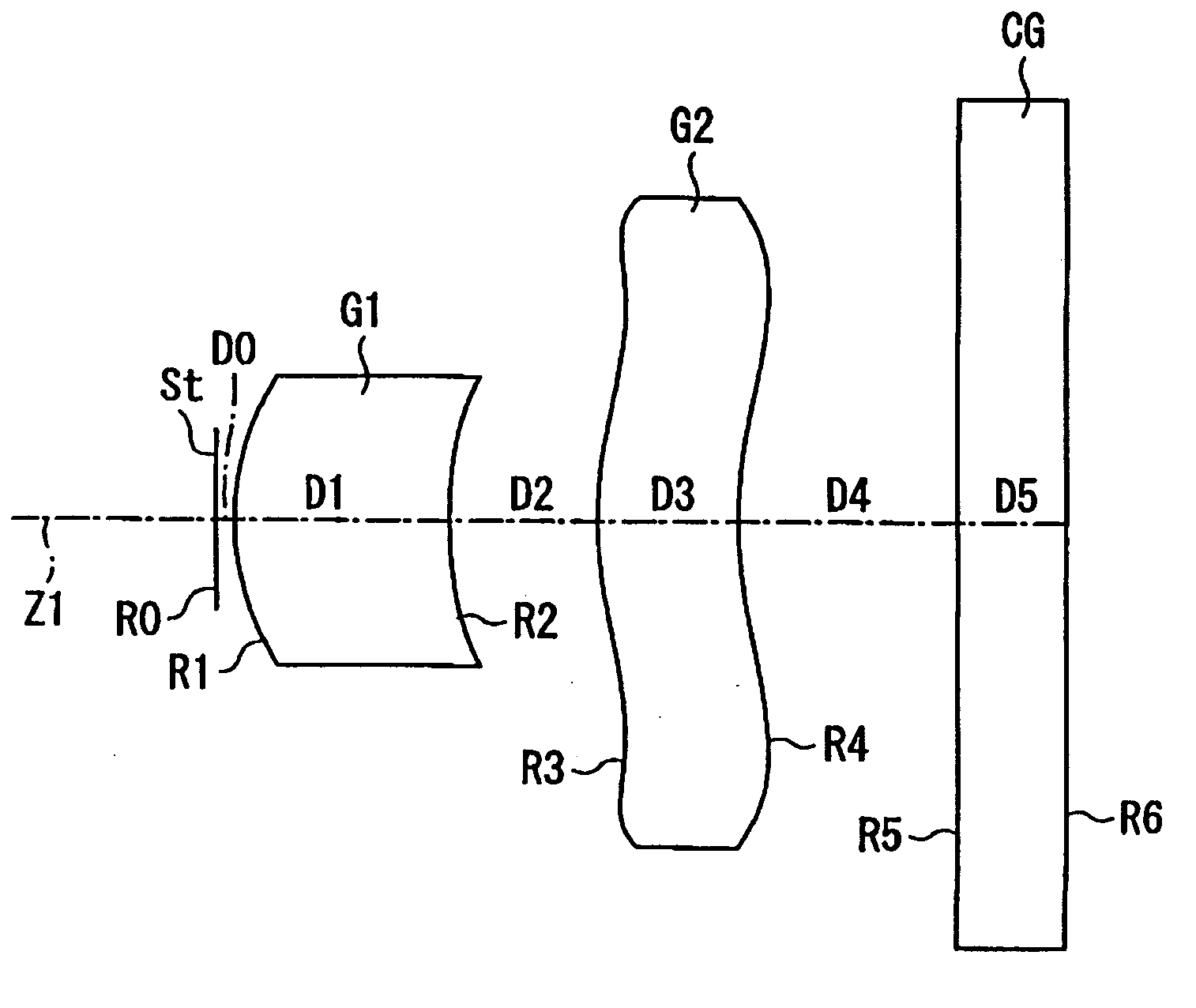
FIG. 1 shows Embodiment 1 of the present invention. Table 1 below lists the surface number #, in order from the object side, the radius of curvature R (in mm) of each surface near the optical axis, the on-axis surface spacing D (in mm), as well as the refractive index Nd and the Abbe number νd (both at the d-line of 587.6 nm) of each optical element for Embodiment 1. Listed in the bottom portion of Table 1 are the focal length f on the optical axis of the entire single focus lens, the f-number FNO, and the maximum field angle 2ω.

TABLE 1#RDNdνd0 (stop)∞0.101*1.46381.181.5061456.42*2.34640.823*2.09050.771.5061456.44*2.74661.185∞0.601.5168064.26∞

f = 3.94 mm FNO = 4.0 2ω = 60.7°

The surfaces with a* to the right of the surface number in Table 1 are aspheric lens surfaces, and the aspheric surface shapes are expressed by Equation (A) above.

Table 2 below lists the values of the constant K and the aspheric coefficients A3-A10 used in Equation (A) above for each of the aspheric lens sur...

embodiment 2

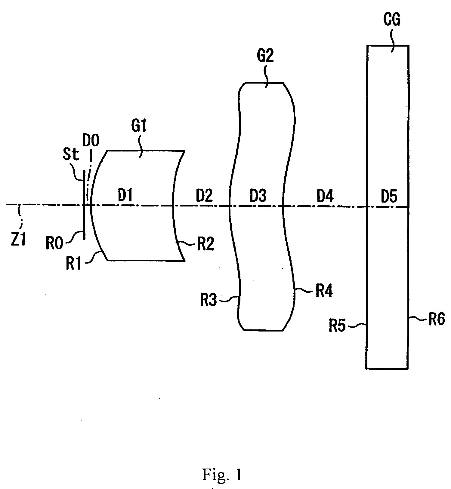
FIG. 2 shows Embodiment 2 of the present invention. Table 4 below lists the surface number #, in order from the object side, the radius of curvature R (in mm) of each surface near the optical axis, the on-axis surface spacing D (in mm), as well as the refractive index Nd and the Abbe number νd (both at the d-line of 587.6 nm) of each optical element for Embodiment 2. Listed in the bottom portion of Table 4 are the focal length f on the optical axis of the entire single focus lens, the f-number FNO, and the maximum field angle 2ω.

TABLE 4#RDNdνd0 (stop)∞0.101*1.45861.201.4902357.52*2.34800.813*2.09140.761.4902357.54*2.74891.305∞0.601.5168064.26∞

f = 4.08 mm FNO = 4.0 2ω = 58.9°

The surfaces with a*to the right of the surface number in Table 4 are aspheric lens surfaces, and the aspheric surface shapes are expressed by Equation (A) above.

Table 5 below lists the values of the constant K and the aspheric coefficients A3-A10 used in Equation (A) above for each of the aspheric lens surf...


PUM


Abstract

An optical system satisfies conditions related to the optical distortion at the maximum image height and at eighty and sixty percent of the maximum image height in order to reduce the actual observed distortion of an image, for example, an image on a monitor, by balancing the optical distortion with TV distortion. The optical system may be a single focus lens that includes, in order from the object side: a diaphragm stop; and first and second lens components. An aspheric equation that includes a nonzero aspheric coefficient of order three or higher may determine an aspheric shape of a lens surface of the second lens component. Both lens components may be made of plastic.

Description

BACKGROUND OF THE INVENTION In recent years, along with the popularization of personal computers into homes, digital still cameras (hereinafter referred to simply as digital cameras) that enable input of picture image information, such as photographed landscapes and portraits, into a personal computer are rapidly becoming more popular. Additionally, with enhancements in portable telephone functions, portable cameras that include compact imaging modules are rapidly becoming more popular. Additionally, including an imaging module in compact information terminal equipment, such as PDAs (Personal Digital Assistants), is becoming popular. In such devices that include an imaging function, an image pickup element, such as a CCD (Charge Coupled Device) or a CMOS (Complementary Metal Oxide Semiconductor), is used to provide the imaging function. Recently, advancements in the miniaturization of such image pickup elements have been rapidly increasing. This has resulted in a desire for the ma...

Claims


Application Information

Patent Timeline
IPC IPC(8): G02B9/04G02B13/00G02B13/18G02B27/00H04N5/225
CPCG02B9/04G02B27/0025G02B13/18G02B13/003
Inventor SATO, KENICHI
Owner FUJI PHOTO OPTICAL CO LTD
Why Eureka
Try Eureka