
Method, apparatus, system, method and device for data creating, and program for mounting electronic component

a technology for electronic components and circuit boards, applied in the direction of soldering devices, manufacturing tools,auxillary welding devices, etc., can solve the problems of reducing the quality of the circuit board on which electronic components are mounted, generating bridges between electronic components, and affecting the quality of the circuit board. achieve the effect of improving the self-alignment

Inactive Publication Date: 2005-04-14
PANASONIC CORP
View PDF11 Cites 39 Cited by
  • Summary
  • Abstract
  • Description
  • Claims
  • Application Information

AI Technical Summary

Benefits of technology

[0010] The invention has been made in consideration of such conventional problems. In order to solve the problems, the invention provides an electronic component mounting method and device, an electronic component mounting system, an electronic component mounting data creating method, a mounting data creating device, and a program to be used therein which can effectively utilize a self-alignment effect even if the mounting interval of an electronic component is small.

Problems solved by technology

The “solder elevation” causes the “extension wetting” which causes generation of bridges between electronic components.
Therefore, in the case in which the printing position of the solder paste is shifted from the position of the land, there is a problem in that a failure in soldering is occurred after the reflow process. FIG. 31(a) shows a state in which the electronic component is mounted, in alignment with the center position of each land, on the circuit board having the solder paste printed with a shift from the position of the land. FIG. 31(b) shows a result obtained by carrying out the reflow process over the circuit board.
As a result, the solder unnecessarily floods over the side surface of the terminal of the electronic component so that a bridge is generated between the adjacent electronic components or terminals.
However, the bridges are generated frequently in the circuit board having small intervals between the electronic components particularly that causes a remarkable decline in quality of the circuit board on which is mounted electronic components.
However, it is hard to uniformly carry out alignment over the whole circuit board having small mounting internals of electronic components, and substantially, it is very hard to completely correct a local shift.

Method used


Image

  • Method, apparatus, system, method and device for data creating, and program for mounting electronic component
  • Method, apparatus, system, method and device for data creating, and program for mounting electronic component
  • Method, apparatus, system, method and device for data creating, and program for mounting electronic component

Examples


second embodiment

[0142] Next, description will be given to the electronic component mounting method according to the invention.

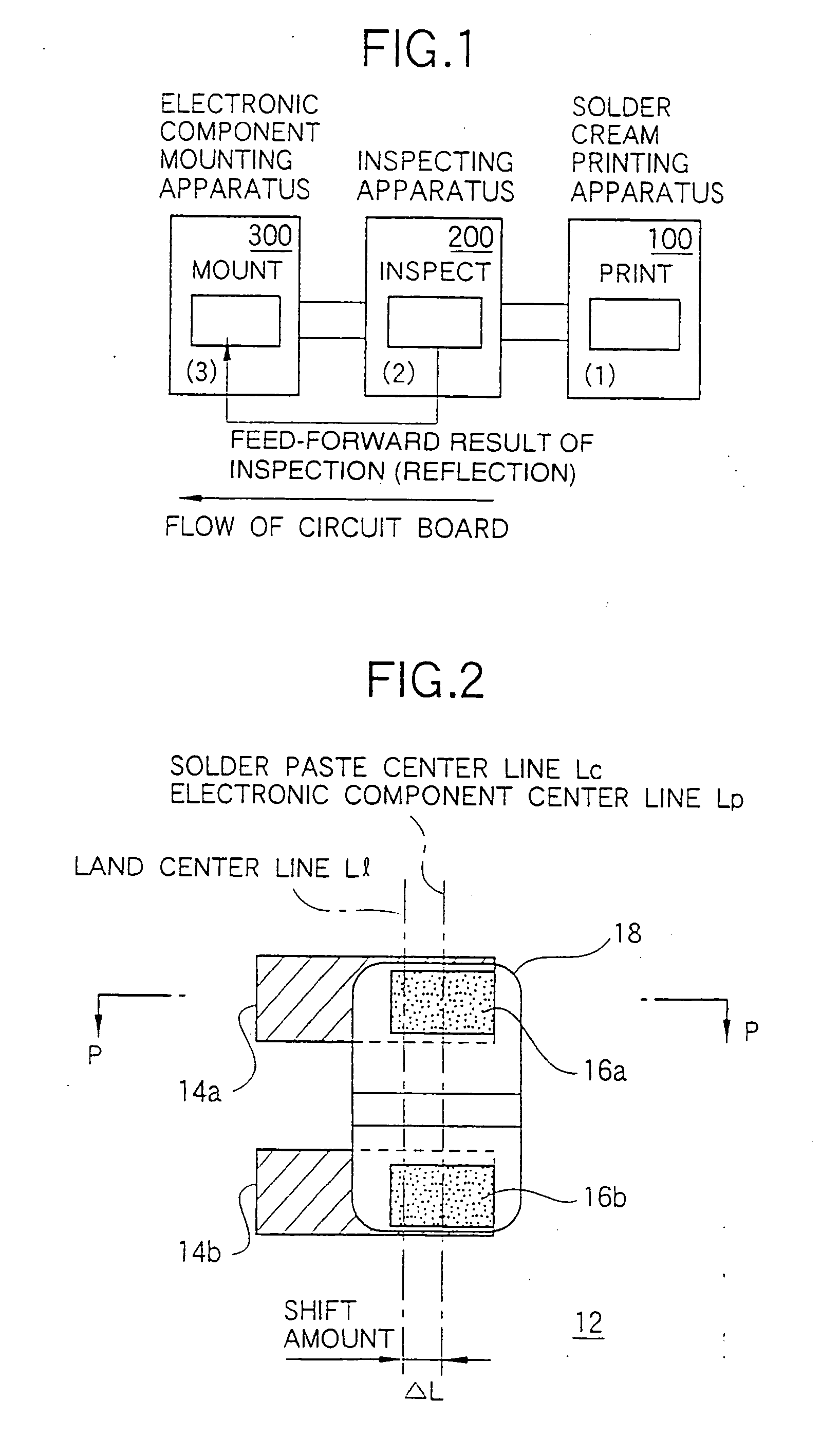
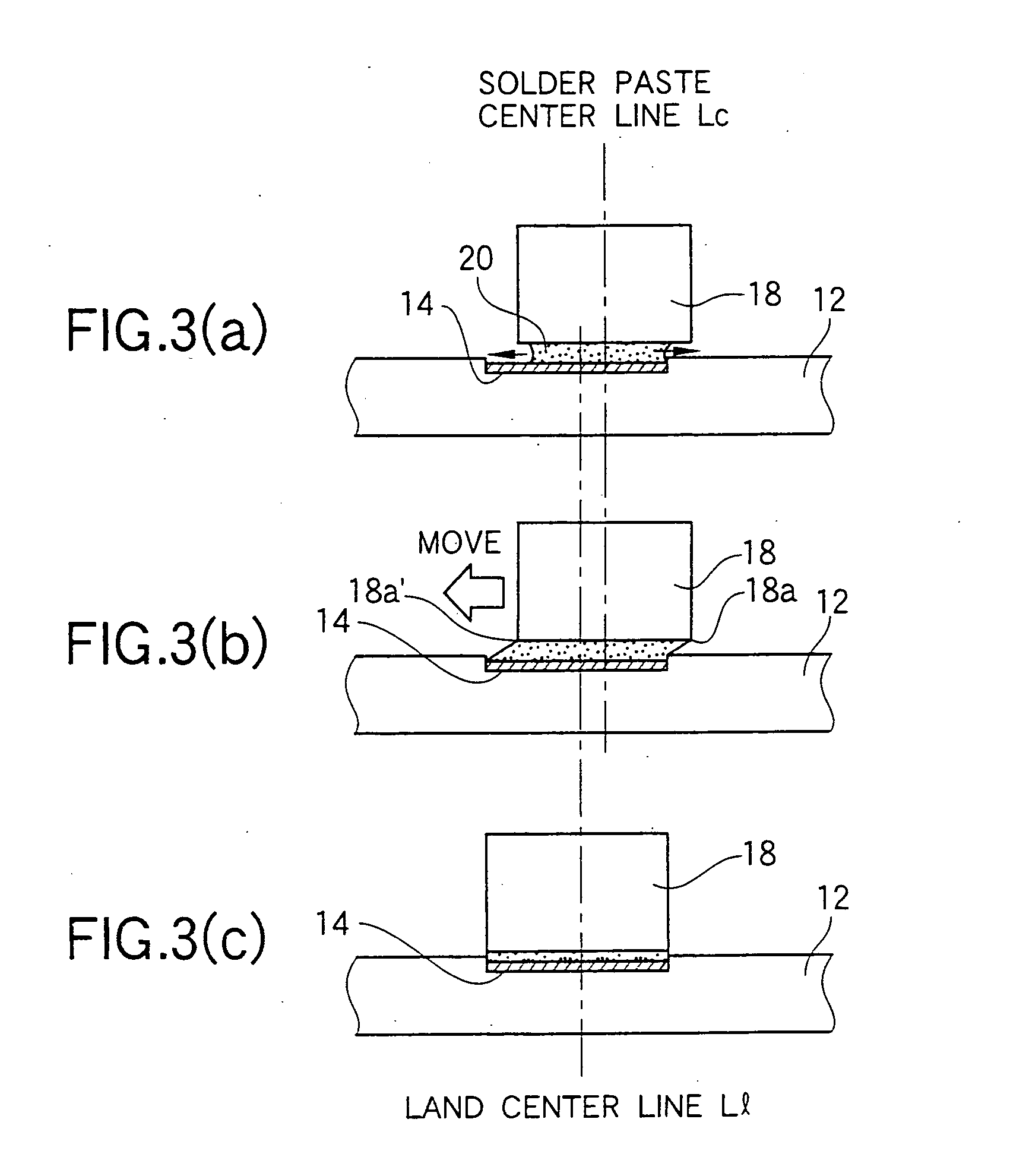
[0143] While the position of the land and the printing position of the solder paste are detected every electronic component for each electronic component to be mounted on the circuit board and the shift amounts thereof are obtained to change the mounting position of the electronic component in the first embodiment, a shift amount between the position of a land and the position of a printed solder paste is obtained for all the electronic components to be mounted on the circuit board and an average value of the shift amount for each electronic component is calculated to collectively change the mounting position of the electronic component on the circuit board based on the average value of the shift amount thus obtained in the second embodiment.

[0144] A specific changing procedure will be described below. For example, in the case in which N electronic components are to be moun...

third embodiment

[0152] Next, description will be given to the electronic component mounting method according to the invention.

[0153] While the amount of the shift of the solder paste printed on the circuit board from the land is averaged and the target mounting position is changed in one way with respect to all the electronic components in the second embodiment, the circuit board is divided into the optional number of blocks, and the average value of a shift amount is obtained for each block and the mounting position of the electronic component is changed for each block by using the average value of each block thus obtained in the third embodiment.

[0154] A pattern for dividing the circuit board into the optional number of blocks includes a dividing pattern shown in FIG. 18, for example. FIG. 18(a) shows an example in which the circuit board is divided annularly into regions from the peripheral edge of the circuit board toward a center and FIG. 18(b) shows an example in which the circuit board is d...

fourth embodiment

[0158] Next, description will be given to the electronic component mounting method according to the invention.

[0159] In the embodiment, as shown in FIG. 19, various parameters such as the weight and shape of an electronic component to be mounted, the material composition of a solder paste to be used, a friction property, a viscosity, a solder powder size, a melting point, a flux component (a resin base, an organism base and an inorganism base), a flux activity or a printing thickness are arranged in a table and a self-alignment ratio is assumed depending on the combination of the type of an electronic component to be actually used and the material of the solder paste by utilizing the table. The self-alignment ratio represents an index indicating, as a percentage, the degree of a shift from the center of the printed solder paste that self-alignment is effective. Based on the self-alignment ratio, the degree (for example, 50%, 80% or 100%) of the shift amount of the printing position ...


PUM


Abstract

This invention provides an electronic component mounting method capable of effectively utilizing a self-alignment effect even if a mounting interval of electronic components is small. This method includes the steps of detecting a printing position of a solder paste on the circuit board and mounting an electronic component. This invention further provides apparatus, devices, and system using the method. When a solder paste on a circuit board having a land formed thereon is printed and an electronic component is mounted, the printing position of the solder paste of the circuit board is detected by a printing position detecting device included in an inspecting apparatus. Then, the electronic component is mounted by using the detected printing position of the solder paste as a reference by an electronic component mounting apparatus.

Description

BACKGROUND OF THE INVENTION [0001] 1. Field of the Invention [0002] The present invention relates to an electronic component mounting method and apparatus for mounting an electronic component on a circuit board with high precision, an electronic component mounting system, an electronic component mounting data creating method, a mounting data creating device, and a program to be used therein. More particularly, the invention relates to a technique for carrying out mounting by effectively utilizing a self-alignment effect without a failure in mounting even if there is a small interval between mounting positions of electronic components on the circuit board. [0003] 2. Description of the Related Art [0004] As shown in FIG. 29, for example, the process for manufacturing a circuit board on which an electronic component mounted includes three steps. The first step is a printing step (1) of printing a solder paste on a circuit board having a land formed thereon by means of a solder paste pr...

Claims


Application Information

Patent Timeline
IPC IPC(8): H05K13/08H05K13/04
CPCH05K13/08H05K13/0465Y10T29/49133Y10T29/49131Y10T29/49149Y10T29/4913Y10T29/49144H05K13/0817
Inventor NAGAFUKU, NOBUYASUNISHIKAWA, NOBORUKURIBAYASHI, TAKESHI
Owner PANASONIC CORP
Features
  • Generate Ideas
  • Intellectual Property
  • Life Sciences
  • Materials
  • Tech Scout
  • Unparalleled Data Quality
  • Higher Quality Content
  • 60% Fewer Hallucinations
Learn More