Fully depleted silicon-on-insulator CMOS logic

Active Publication Date: 2005-04-14
MICRON TECH INC
View PDF99 Cites 56 Cited by
  • Summary
  • Abstract
  • Description
  • Claims
  • Application Information

AI Technical Summary

Benefits of technology

[0010] The above-mentioned problems with adverse floating body effects and other problems are addresse

Problems solved by technology

However, as transistors are made smaller and faster, delays through the connections between the transistors becomes greater in relation to the speed of the transistor.
SOI technology, however, imposes significant technical challenges.
It is very difficult to make perfect crystalline silicon-on-oxide or silicon with other insulators since the insulator layer's crystalline properties are so different from the pure silicon.
If perfect crystalline silicon is not obtained, defects wi

Method used


Image

  • Fully depleted silicon-on-insulator CMOS logic
  • Fully depleted silicon-on-insulator CMOS logic
  • Fully depleted silicon-on-insulator CMOS logic

Examples


Embodiment Construction

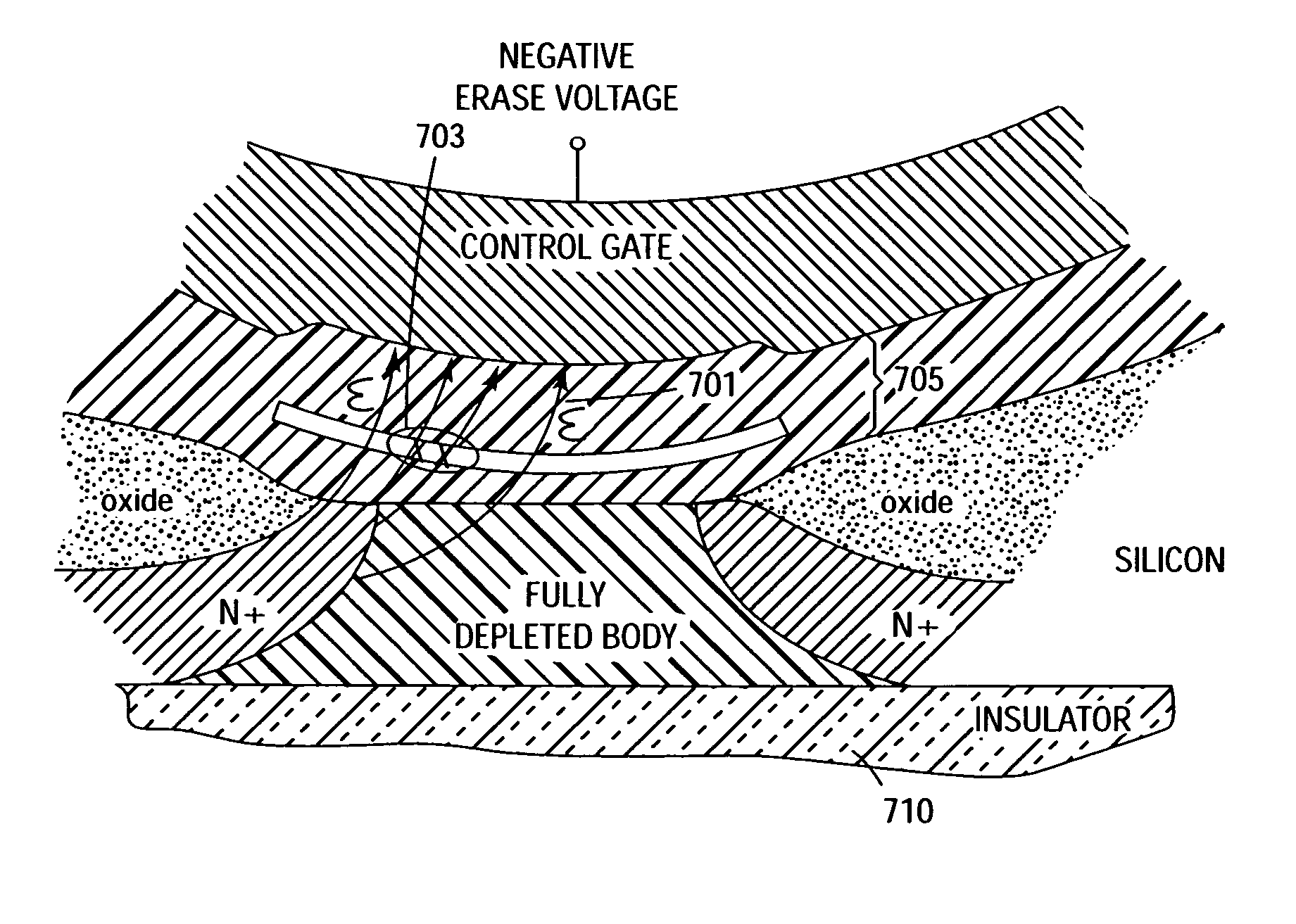
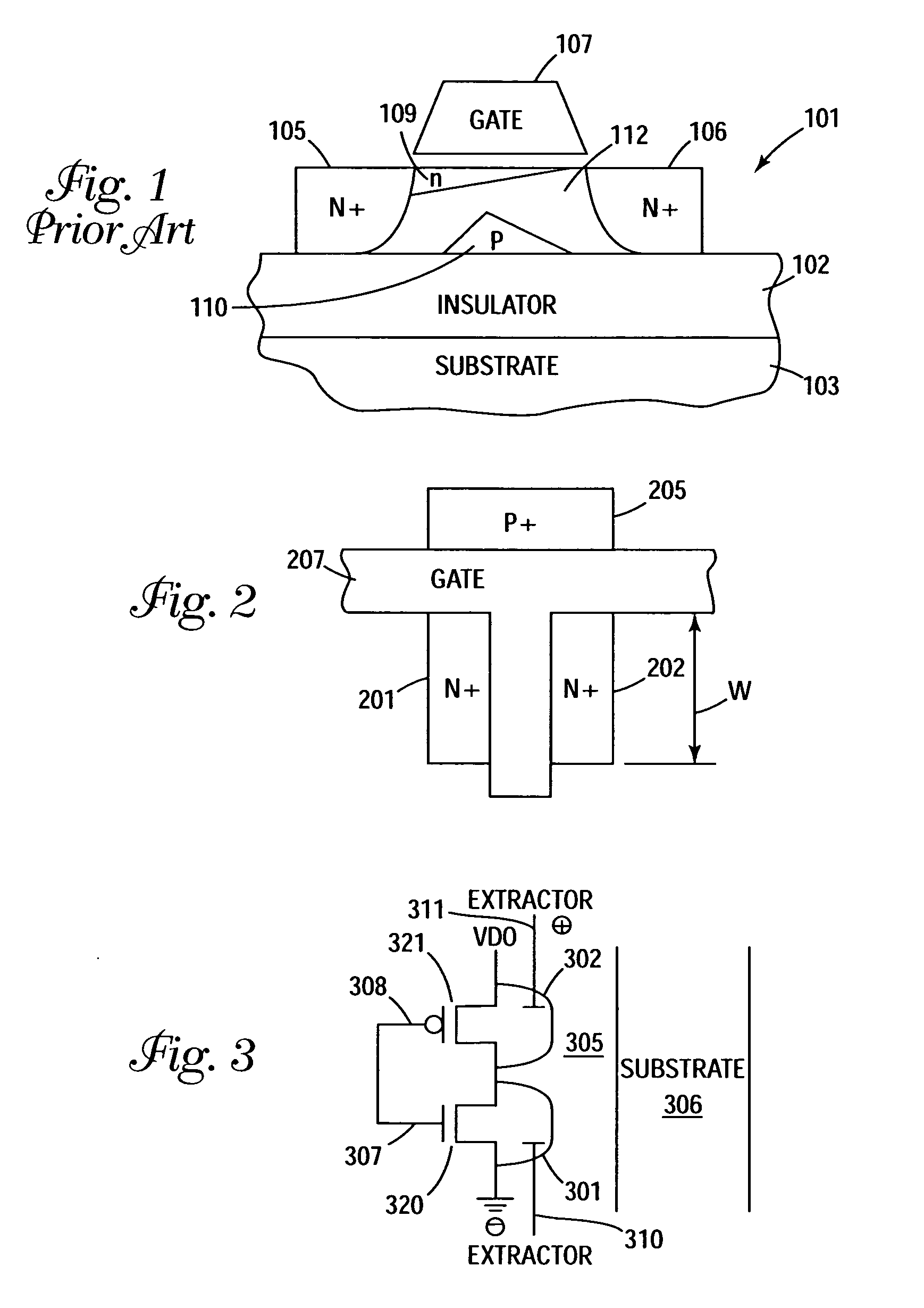
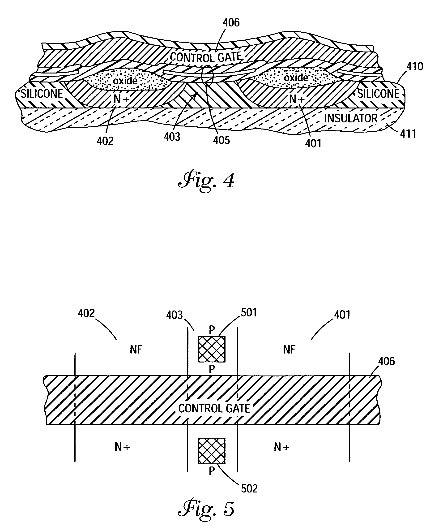
[0022] In the following detailed description of the invention, reference is made to the accompanying drawings that form a part hereof, and in which is shown, by way of illustration, specific embodiments in which the invention may be practiced. In the drawings, like numerals describe substantially similar components throughout the several views. These embodiments are described in sufficient detail to enable those skilled in the art to practice the invention. Other embodiments may be utilized and structural, logical, and electrical changes may be made without departing from the scope of the present invention. The following detailed description is, therefore, not to be taken in a limiting sense, and the scope of the present invention is defined only by the appended claims and equivalents thereof.

[0023]FIG. 2 illustrates a top view of one embodiment of a silicon-on-insulator (SOI) NMOS transistor of the present invention. The present invention uses reverse biasing of the body contacts,...


PUM


Abstract

A extractor implanted region is used in a silicon-on-insulator CMOS memory device. The extractor region is reversed biased to remove minority carriers from the body region of partially depleted memory cells. This causes the body region to be fully depleted without the adverse floating body effects.

Description

RELATED APPLICATIONS [0001] This is a divisional application of U.S. patent application Ser. No. 10 / 682,590 filed Oct. 9, 2003, titled “Fully Depleted Silicon-On-Insulator CMOS Logic” and commonly assigned, the entire contents of which is incorporated herein by reference.TECHNICAL FIELD OF THE INVENTION [0002] The present invention relates generally to silicon-on-insulator devices and in particular the present invention relates to fully depleted silicon-on-insulator logic. BACKGROUND OF THE INVENTION [0003] The increased speed and capability of computers and other electronic devices requires better performance from the integrated circuits that make up a device. One way to make the integrated circuits faster is to reduce the size of the transistors that make up the device. However, as transistors are made smaller and faster, delays through the connections between the transistors becomes greater in relation to the speed of the transistor. [0004] An alternative technique to speed up in...

Claims


Application Information

Patent Timeline
IPC IPC(8): G11C16/04H01L21/00H01L21/28H01L21/336H01L29/76H01L29/786H01L29/792
CPCG11C16/0475G11C2211/4016H01L21/28282H01L21/84H01L27/115H01L27/11568H01L29/7926H01L29/66833H01L29/7848H01L29/78615H01L29/792H01L29/7923H01L27/1203H01L29/40117H10B43/30H10B69/00
Inventor FORBES, LEONARD
Owner MICRON TECH INC
Why Eureka
Try Eureka