Discharge display apparatus minimizing addressing power and method of driving the same

a technology of addressing power and display apparatus, which is applied in the direction of identification means, instruments, light sources, etc., can solve the problems of reducing the brightness of light emitted from a pdp, and affecting the operation of the circuit. , to achieve the effect of reducing the consumption of power and improving the operation of the circui

Inactive Publication Date: 2005-04-14
SAMSUNG SDI CO LTD
View PDF18 Cites 16 Cited by
  • Summary
  • Abstract
  • Description
  • Claims
  • Application Information

AI Technical Summary

Benefits of technology

[0018] It is therefore and objective of present invention to provide a discharge display apparatus which improves the operation of a circuit for recovering addressing power to decrease consumed power without distortion of the waveform of an addressing voltage, and a method of driving the discharge display apparatus.
[0019] It is another object to provide in the discharge display apparatus and the method of driving the same according to the present invention, the operational timing of a power recovery circuit varying in response to display data signals applied to address electrode lines, and as a result, the operational timing of the power recovery circuit becomes proper for a variable capacitance of a discharge display panel so that the waveform of an addressing voltage is not distorted and consumed power decreases.
[0020] It is yet another object of the present invention to provide a discharge display apparatus and method that is easy to implement, cost effective, reliable and efficient.
[0023] According to the discharge display apparatus and the method of driving the same, the operational timing of the power recovery circuit varies in response to display data signals applied to the address electrode lines. As such, the operational timing of the power recovery circuit becomes proper for variable capacitance of the discharge display panel such that the waveform of the addressing voltage is not distorted and consumed power decreases.

Problems solved by technology

As such, a time taken for the address periods with respect to each sub-field becomes long and the display periods become short, causing degradation of the brightness of light emitted from a PDP.
As a result, the operational timing of the power recovery circuit is improper for a capacitance of the discharge display panel so that the waveform of an addressing voltage is distorted and consumed power increases.

Method used


Image

  • Discharge display apparatus minimizing addressing power and method of driving the same
  • Discharge display apparatus minimizing addressing power and method of driving the same
  • Discharge display apparatus minimizing addressing power and method of driving the same

Examples


Embodiment Construction

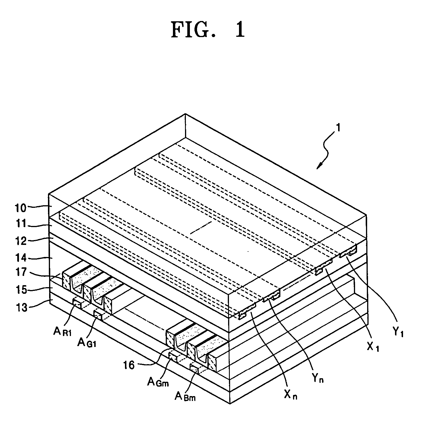
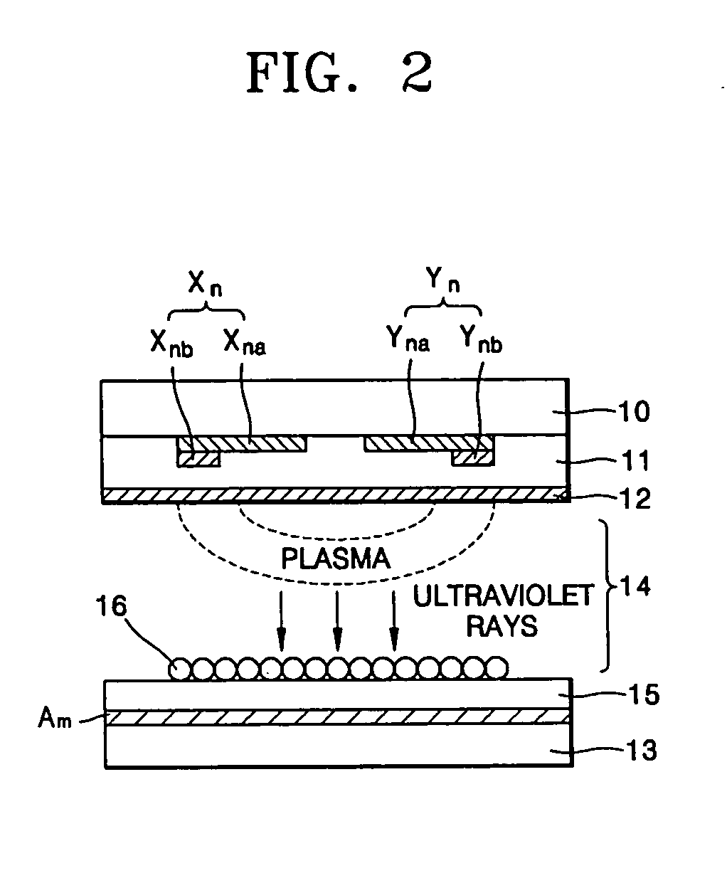
[0034] Turning now to the drawings, FIG. 1 shows the structure of a plasma display panel (PDP) as a conventional discharge display panel. FIG. 2 shows an example of a display cell of the plasma display panel of FIG. 1. Referring to FIGS. 1 and 2, address electrode lines AR1, AG1, . . . , AGm, and ABm, dielectric layers 11 and 15, Y-electrode lines Y1, . . . , and Yn, X-electrode lines X1, . . . , and Xn, a fluorescent layer 16, partition walls 17, and an MgO layer 12 as a protection layer are disposed between front and rear glass substrates 10 and 13 of a conventional surface-discharge plasma display panel (PDP) 1.

[0035] The address electrode lines AR1, AG1, . . . , AGm, and ABm are formed at a front side of the rear glass substrate 13 in the form of a predetermined pattern. The entire surface of the lower dielectric layer 15 is coated in the front of the address electrode lines AR1, AG1, . . . , AGm, and ABm. The partition walls 17 are formed at a front side of the lower dielectri...


PUM


Abstract

A discharge display apparatus includes a discharge display panel; a controller; an address driver, which generate display data signals by processing an address signal generated by the controller and applies the display data signals to address electrode lines of the discharge display panel; and a power recovery circuit of the address driver, where operational timing of the power recovery circuit varies in response to the display data signals applied to the address electrode lines.

Description

CLAIM OF PRIORITY [0001] This application makes reference to, incorporates the same herein, and claims all benefits accruing under 35 U.S.C. §119 from an application for DISCHARGE DISPLAY APPARATUS MINIMIZING ADDRESSING POWER, AND METHOD FOR DRIVING THE APPARATUS earlier filed in the Korean Intellectual Property Office on 14 Oct. 2003 and there duly assigned Serial No. 2003-71452. BACKGROUND OF THE INVENTION [0002] 1. Field of the Invention [0003] The present invention relates to a discharge display apparatus and a method of driving the same, and more particularly, to a discharge display apparatus having an addressing power recovery circuit and a method of driving the same. [0004] 2. Description of the Related Art [0005] A plasma display panel (PDP) as a conventional discharge display panel includes display cells of the plasma display panel. Address electrode lines, dielectric layers, Y-electrode lines, X-electrode lines, a fluorescent layer, partition walls, and an MgO layer as a p...

Claims


Application Information

Patent Timeline
Patent Type & Authority Applications(United States)
IPC IPC(8): G09F9/313G09G3/28G09G3/10G09G3/288H01J17/49
CPCG09G3/293G09G3/2965G09G2360/16G09G2310/066G09G2310/0216G09G3/296
Inventor JIN, KWANG-HOKIM, JIN-SUNG
Owner SAMSUNG SDI CO LTD
Why Eureka
Try Eureka