Semiconductor device and method of fabricating the same
a technology of semiconductor devices and mosfets, which is applied in the direction of semiconductor devices, semiconductor/solid-state device details, electrical apparatus, etc., can solve the problems of failure to keep a desirable drain voltage resistance level, punching through between the source and the drain, and more likely failure to achieve the desired drain voltage resistance. , to achieve the effect of suppressing the reduction of drain voltage resistance and lowering the drain resistan
- Summary
- Abstract
- Description
- Claims
- Application Information
AI Technical Summary
Benefits of technology
Problems solved by technology
Method used
Image
Examples
first embodiment
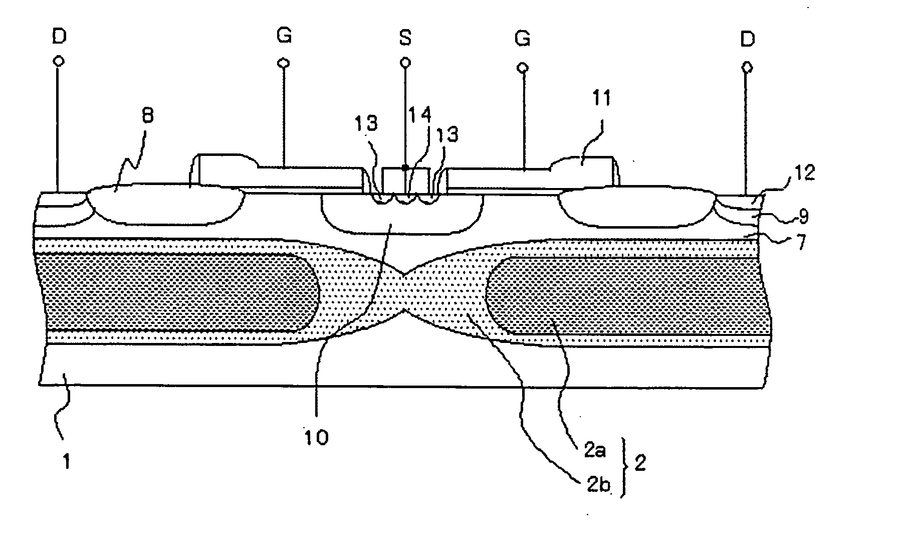
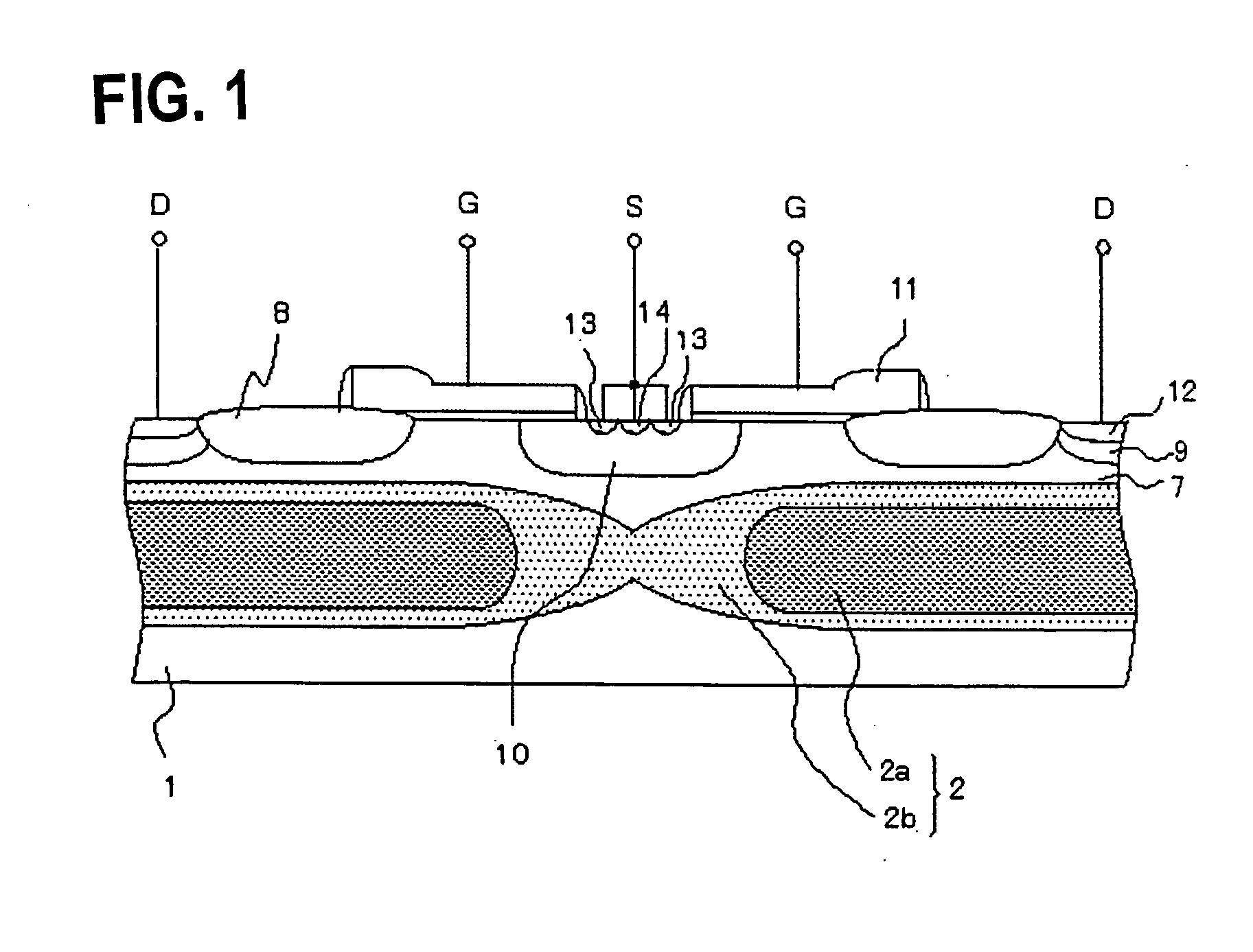
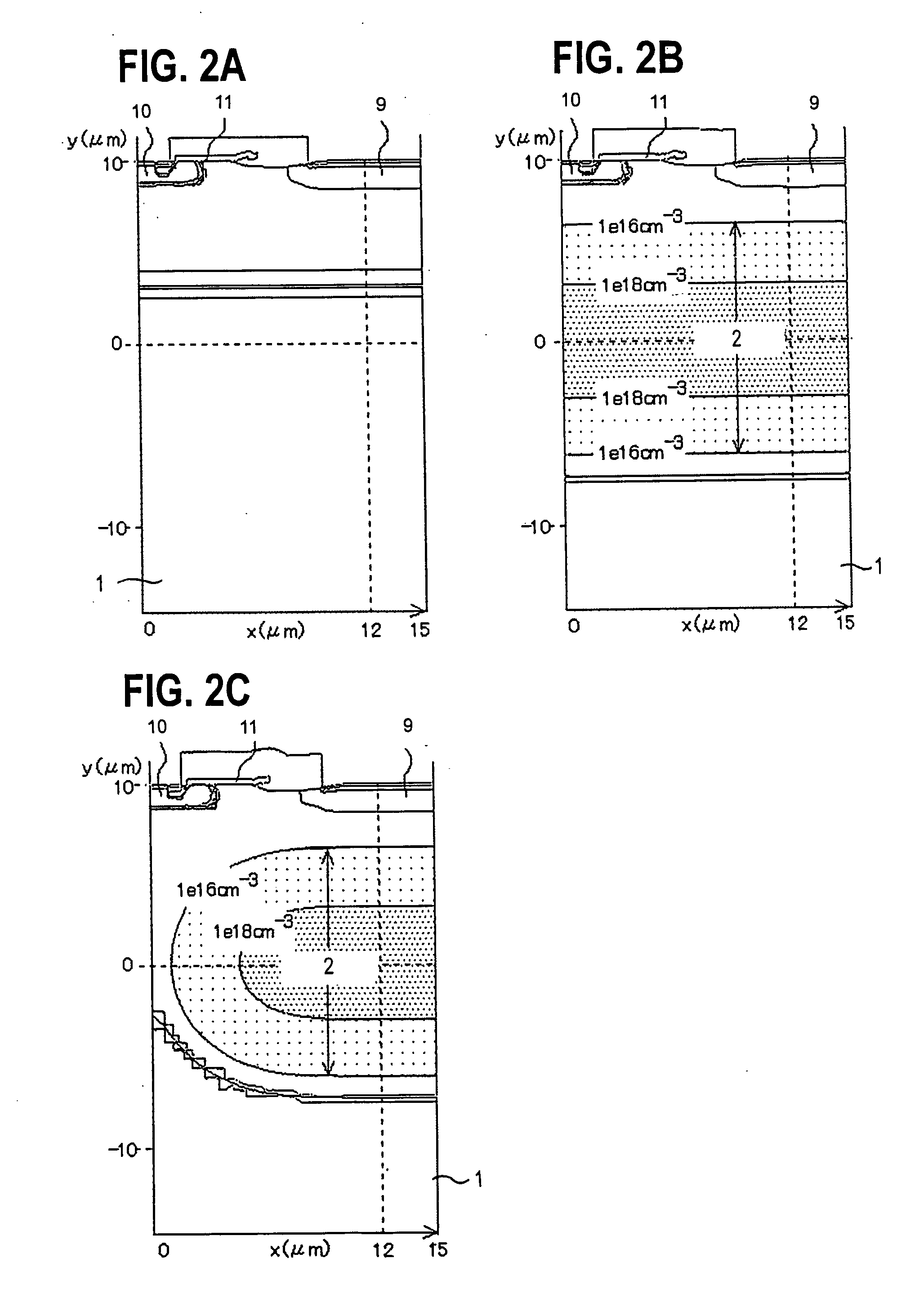
[0049] To further detail the aforementioned present invention, a DMOSFET and a method of fabricating the same according to a first mode of embodiment of the present invention will be described below, referring to FIG. 1 to FIG. 16B. FIG. 1 is a drawing showing a structure of the DMOSFET of the present invention, FIGS. 2A to 3B are drawings showing a profile of the N-type buried layer in the DMOSFET according to this mode of embodiment, FIGS. 4 to 12 are sectional views showing process steps of the method of fabricating the DMOSFET according to this mode of embodiment, and FIGS. 13 to 16B are drawings showing effects of the DMOSFET of the this mode of embodiment.
[0050] As shown in FIG. 1, the DMOSFET of this mode of embodiment has an N-type buried layer 2, formed on a P-type semiconductor substrate 1, of which impurity concentration varied in the in-plane direction of the substrate, and has a drain region 7 composed of an epitaxial layer formed on the N-type buried layer 2. The drai...
second embodiment
[0068] A DMOSFET and a method of fabricating the same according to a second embodiment of the present invention will be described below, referring to FIGS. 17 to 24. FIGS. 17 to 23 are sectional views showing process steps of the method of fabricating the DMOSFET according to the second embodiment, and FIG. 24 is a sectional view showing a structure of the DMOSFET according to the second embodiment. Although in the aforementioned first embodiment, the P-type epitaxial layer 4 is grown, and the drain region 7 is then formed by embedding the N-type impurity into the P-type epitaxial layer 4, it is also possible to form the N-type epitaxial layer directly on the N-type, heavily-doped buried layers 2a. Based on the idea, a method of fabrication in this case will be explained in the second embodiment, referring to FIGS. 17 to 23.
[0069] First, as shown in FIG. 17, the mask 3 typically composed of a silicon oxide film is formed on the P-type semiconductor substrate 1, so as to cover at le...
PUM
 Abstract
Description
Claims
Application Information


