Method and apparatus for thermo-optic modulation of optical signals
- Summary
- Abstract
- Description
- Claims
- Application Information
AI Technical Summary
Benefits of technology
Problems solved by technology
Method used
Image

Examples
Embodiment Construction
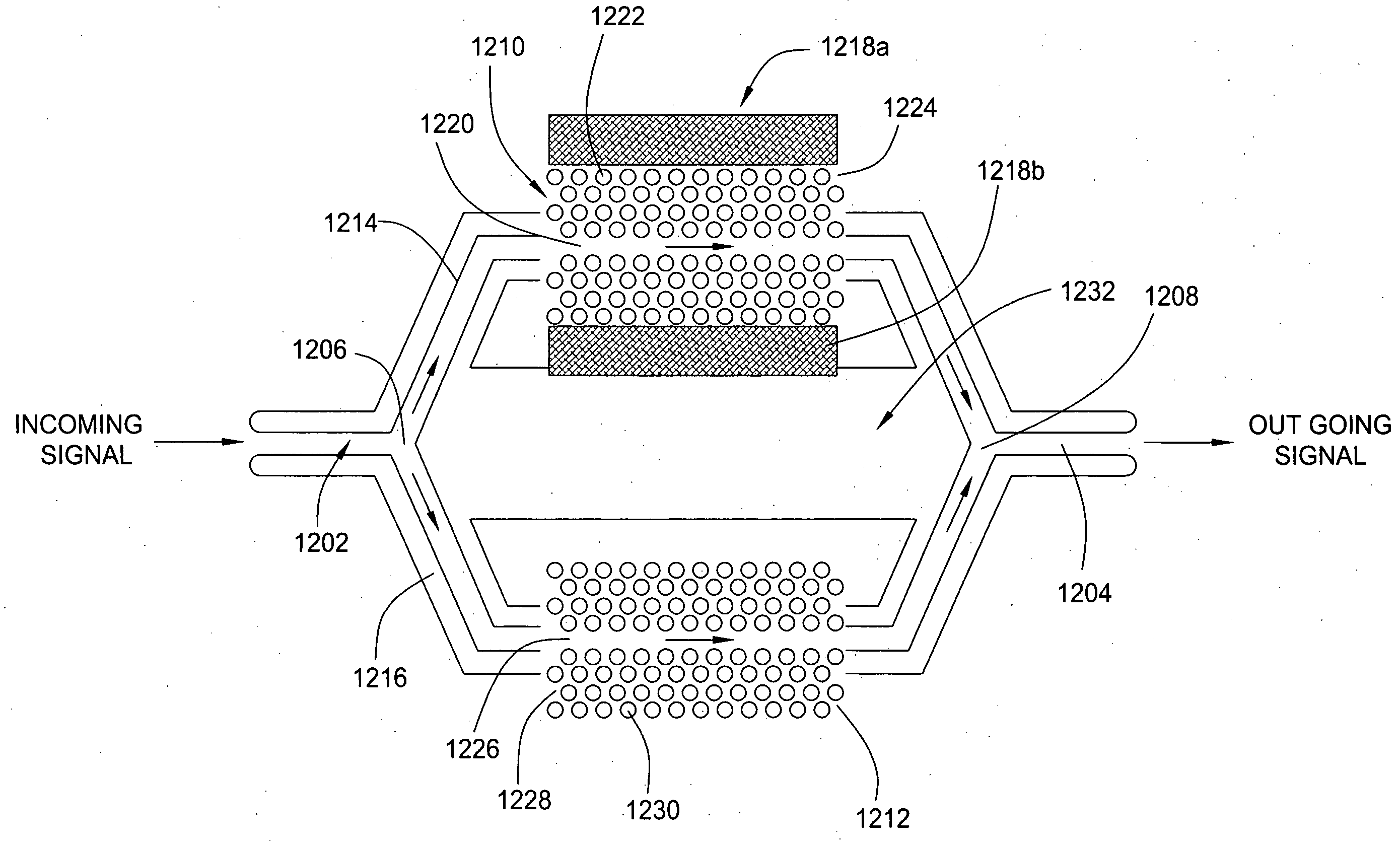
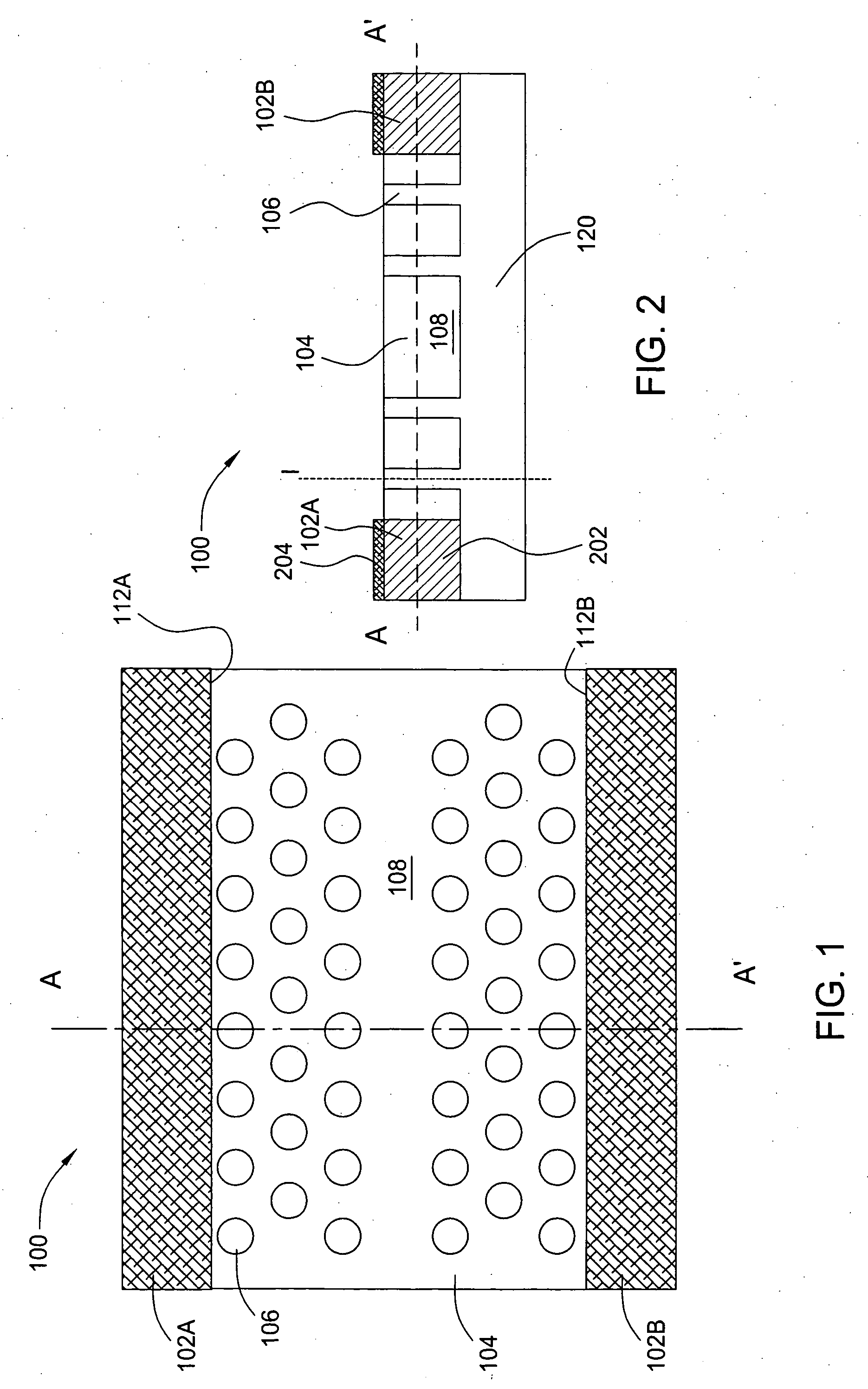
[0025]FIG. 1 is a top plan view of one embodiment of a two-dimensional photonic crystal waveguide structure 100 with lateral contacts 102a and 102b (hereinafter collectively referred to as “contacts 102”) according to the present invention. The photonic crystal structure 100 comprises a substrate 104, a plurality of apertures 106 formed in the substrate 104, a linear defect, e.g., a waveguide 108, and first and second lateral electrical contacts 102a and 102b. As illustrated in FIG. 2, which is a cross-sectional view of the photonic crystal structure 100 taken along line A-A′ of FIG. 1, the apertures 106 extend substantially completely through the substrate 104 (i.e., like channels) to an optical isolation layer 120, and the apertures 106 are arranged in rows to form a periodic lattice. The waveguide 108 is positioned to form a sort of channel through the lattice structure, with several rows of apertures 106 extending outward from the longitudinal edges of the waveguide 108. The fir...
PUM
 Abstract
Description
Claims
Application Information
 - R&D
- Intellectual Property
- Life Sciences
- Materials
- Tech Scout
- Unparalleled Data Quality
- Higher Quality Content
- 60% Fewer Hallucinations
Browse by: Latest US Patents, China's latest patents, Technical Efficacy Thesaurus, Application Domain, Technology Topic, Popular Technical Reports.
© 2025 PatSnap. All rights reserved.Legal|Privacy policy|Modern Slavery Act Transparency Statement|Sitemap|About US| Contact US: help@patsnap.com