Method and apparatus for depositing material

a technology of material and evaporation mask, which is applied in the direction of vacuum evaporation coating, electroluminescent light source, coating, etc., can solve the problems of limiting the application of organic semiconductors, limiting the resolution of conventional semiconductor processing methods, and limiting the resolution of organic layers

Active Publication Date: 2005-04-28
THE TRUSTEES FOR PRINCETON UNIV
View PDF18 Cites 114 Cited by
  • Summary
  • Abstract
  • Description
  • Claims
  • Application Information

AI Technical Summary

Problems solved by technology

However, the unique processing requirements of organic semiconductors can also limit their application.
However, the organic layers are typically too fragile to withstand conventional semiconductor processing methods such as photolithography, plasma processing, or reactive ion etching.
However, the resolution that may be achieved with such masks is limited due to a number of factors, including the resolution to which a mask may be reliably fabricated, the buildup of organic material on the mask, and the diffusion of organic material in between the mask and the substrate over which it is being deposited.

Method used


Image

  • Method and apparatus for depositing material
  • Method and apparatus for depositing material
  • Method and apparatus for depositing material

Examples


Embodiment Construction

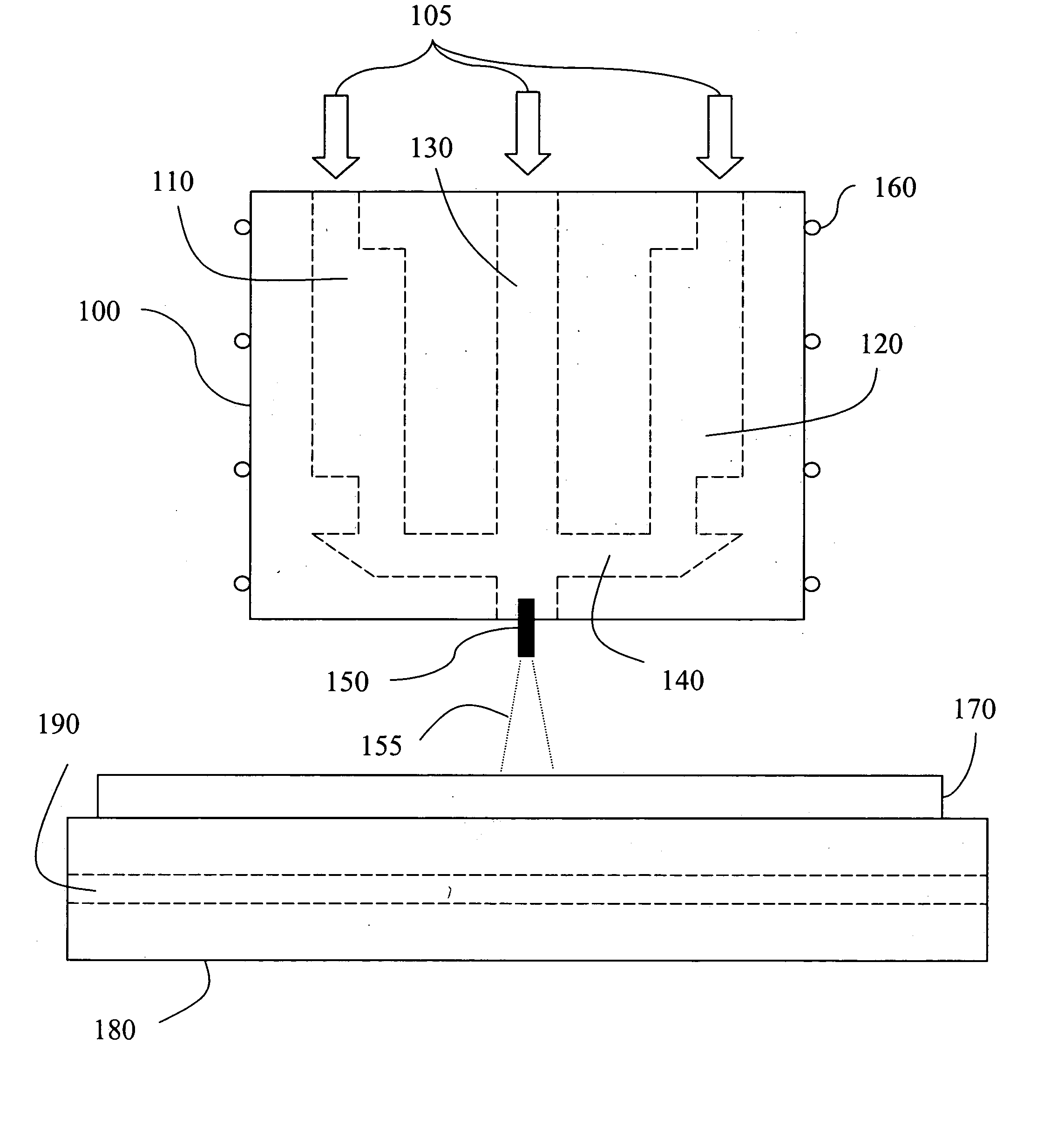
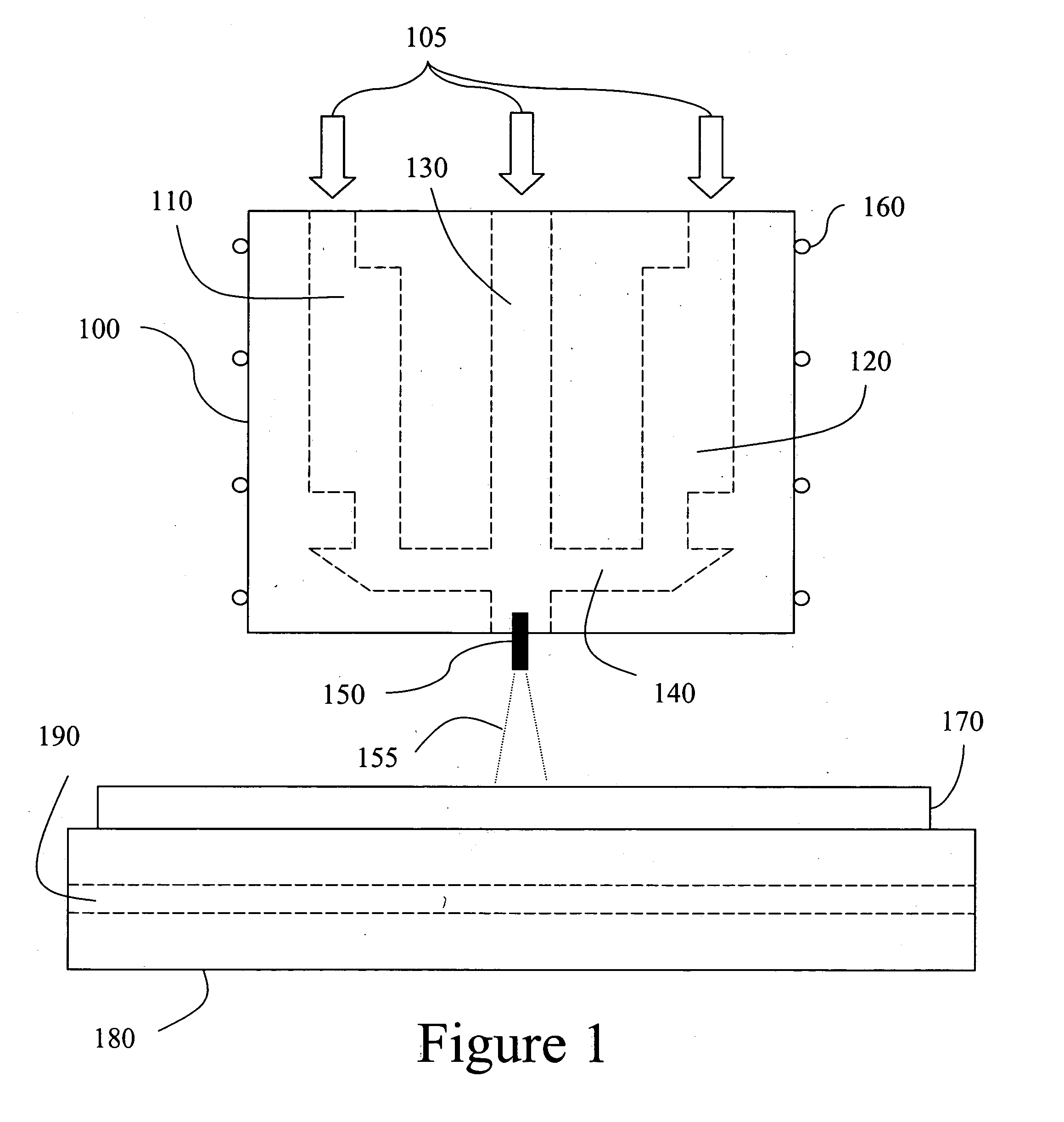
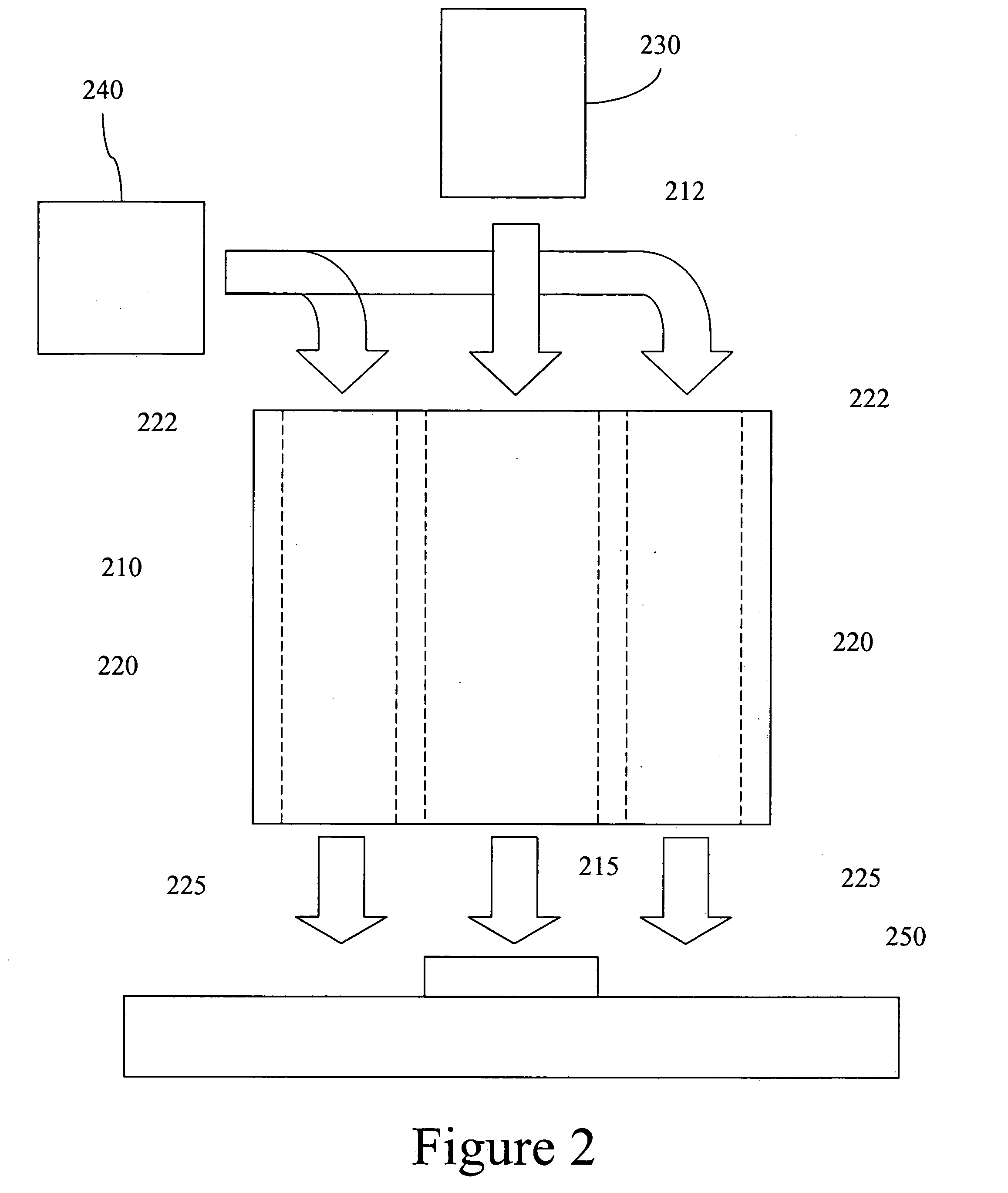
[0024] Organic vapor jet printing (OVJP) is introduced for the direct patterning during growth of molecular organic semiconductor thin films. A hot inert carrier gas picks up organic vapor and expands through a microscopic nozzle, resulting in a highly collimated jet. The jet impinges on a cold substrate, leading to the selective physisorption of the organic molecules but not the carrier gas. The non-equilibrium nature of OVJP allows for high resolution, nearly 100% efficient, direct printing of organic semiconductor patterns and devices. The deposition rates may be very high, for example up to and exceeding 1000 Å / s. We demonstrate pattern resolution determined in part by the nozzle diameter and separation from the substrate. For example, employing a 20 μm diameter orifice, we obtained patterns of ˜25 μm in diameter (1000 dots per inch). Further, we print an archetypal pentacene channel thin film transistor at a film deposition rate of 700 Å / s, resulting in hole mobility of 0.25 cm...


PUM

PropertyMeasurementUnit
dynamic pressureaaaaaaaaaa
pressureaaaaaaaaaa

Abstract

A method of depositing organic material is provided. A carrier gas carrying an organic material is ejected from a nozzle at a flow velocity that is at least 10% of the thermal velocity of the carrier gas, such that the organic material is deposited onto a substrate. In some embodiments, the dynamic pressure in a region between the nozzle and the substrate surrounding the carrier gas is at least 1 Torr, and more preferably 10 Torr, during the ejection. In some embodiments, a guard flow is provided around the carrier gas. In some embodiments, the background pressure is at least about 10e-3 Torr, more preferably about 0.1 Torr, more preferably about 1 Torr, more preferably about 10 Torr, more preferably about 100 Torr, and most preferably about 760 Torr. A device is also provided. The device includes a nozzle, which further includes a nozzle tube having a first exhaust aperture and a first gas inlet; and a jacket surrounding the nozzle tube, the jacket having a second exhaust aperture and a second gas inlet. The second exhaust aperture completely surrounds the first tube aperture. A carrier gas source and an organic source vessel may be connected to the first gas inlet. A guard flow gas source may be connected to the second gas inlet. The device may include an array of such nozzles.

Description

FIELD OF THE INVENTION [0001] The present invention relates to a method and apparatus for depositing material. BACKGROUND [0002] Opto-electronic devices that make use of organic materials are becoming increasingly desirable for a number of reasons. Many of the materials used to make such devices are relatively inexpensive, so organic opto-electronic devices have the potential for cost advantages over inorganic devices. In addition, the inherent properties of organic materials, such as their flexibility, may make them well suited for particular applications such as fabrication on a flexible substrate. Examples of organic opto-electronic devices include organic light emitting devices (OLEDs), organic phototransistors, organic photovoltaic cells, and organic photodetectors. For OLEDs, the organic materials may have performance advantages over conventional materials. For example, the wavelength at which an organic emissive layer emits light may generally be readily tuned with appropriat...

Claims


Application Information

Patent Timeline
Patent Type & Authority Applications(United States)
IPC IPC(8): C23C14/04C23C14/12H01L51/00H01L51/30H01L51/40
CPCC23C14/12H01L51/0081H01L51/0013C23C14/228H10K71/18H10K85/324H05B33/10
Inventor SHTEIN, MAXFORREST, STEPHEN R.MICHELS, JOE
Owner THE TRUSTEES FOR PRINCETON UNIV
Why Eureka
Try Eureka