Thin film transistor substrate for display device and fabricating method thereof

a thin film transistor and substrate technology, applied in the field of thin film transistor substrate for display devices and fabricating methods thereof, can solve the problems of complex process for forming thin film transistor substrates, high cost of semiconductor processes for forming thin film transistors, and the inability to lift off the four-round mask process, so as to achieve the effect of improving lift-off ability and simplifying the process

Active Publication Date: 2005-04-28
LG DISPLAY CO LTD
View PDF13 Cites 32 Cited by
  • Summary
  • Abstract
  • Description
  • Claims
  • Application Information

AI Technical Summary

Benefits of technology

[0027] Accordingly, it is an object of the present invention to provide a thin film transistor substrate for a display device and a fabricating method thereof having a simplified process by using a lift-off process.
[0028] Another object of the present invention is to provide a thin film transistor substrate for a display device and a fabricating method thereof having an improved lift-off ability.

Problems solved by technology

In manufacturing such a liquid crystal display, the process for forming the thin film transistor substrate is complicated and is a major factor in the manufacturing cost of the liquid crystal display panel.
The semiconductor processes for forming the thin film transistor is expensive because it needs a plurality of masking processes.
However, the four-round mask process is still a complicated and expensive fabricating process.

Method used


Image

  • Thin film transistor substrate for display device and fabricating method thereof
  • Thin film transistor substrate for display device and fabricating method thereof
  • Thin film transistor substrate for display device and fabricating method thereof

Examples


Embodiment Construction

[0045] Reference will now be made in detail to the preferred embodiments of the present invention, examples of which are illustrated in the accompanying drawings. Hereinafter, the preferred embodiments of the present invention will be described in detail with reference to FIGS. 4 to 10C.

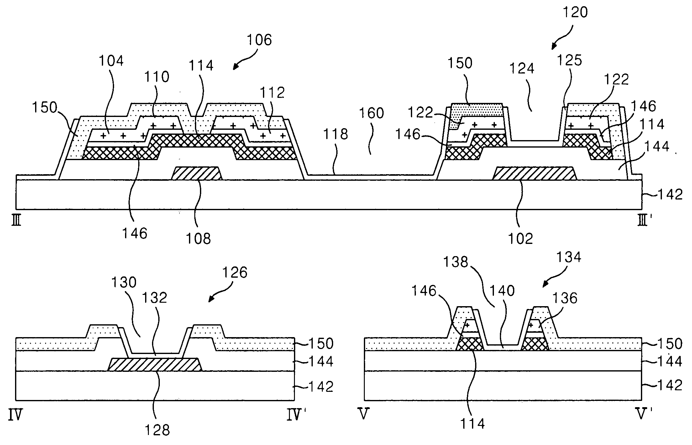
[0046]FIG. 4 is a plan view showing a portion of a thin film transistor substrate according to an embodiment of the present invention, and FIG. 5 is a cross-sectional view of the thin film transistor substrate taken along the III-III′, IV-IV′ and V-V′ lines in FIG. 4. Referring to FIG. 4 and FIG. 5, the thin film transistor substrate includes a gate line 102 and a data line 104 crossing each other on a lower substrate 142 with a gate insulating film 144 between the lower substrate 142 and the lines. A thin film transistor 106 is provided adjacent to a crossing of the gate line 102 and the data line 104. A pixel electrode 118 provided in a pixel area defined by the gate line 102 and the data line 104...


PUM

PropertyMeasurementUnit
areaaaaaaaaaaa
transparentaaaaaaaaaa
transparent conductiveaaaaaaaaaa

Abstract

A thin film transistor substrate for a display device having a plurality of thin film transistors and pixel electrodes connected to the thin film transistors, said thin film transistor substrate includes: a plurality of pad electrodes in a non-display area of the display device for applying signals to the plurality of thin film transistors in a non-display area of the display device; a protective film covering the pad electrodes in the non-display area; and a slit in the protective film adjacent to at least one of the plurality of pad electrodes.

Description

[0001] This application claims the benefit of Korean Patent Application No. P2003-74138 filed in Korea on Oct. 23, 2003, which is hereby incorporated by reference. BACKGROUND OF THE INVENTION [0002] 1. Field of the Invention [0003] This invention relates to a device of a liquid crystal display, and more particularly to a thin film transistor substrate for a display device and a fabricating method thereof. [0004] 2. Description of the Related Art [0005] Generally, a liquid crystal display (LCD) controls light transmittance of a liquid crystal using an electric field to thereby display a picture. The LCD includes a liquid crystal display panel having liquid crystal cells arranged in a matrix, and a driving circuit for driving the liquid crystal display panel. The liquid crystal display panel includes a thin film transistor substrate and a color filter substrate that are opposed to each other, a liquid crystal injected between the two substrates, and a spacer for keeping a cell gap bet...

Claims


Application Information

Patent Timeline
Patent Type & Authority Applications(United States)
IPC IPC(8): G02F1/1368G02F1/1345G02F1/136G02F1/1362G09F9/30G09F9/35H01L21/336H01L21/77H01L21/84H01L21/86H01L27/12H01L29/786
CPCG02F1/1362G02F2001/136231H01L27/1288H01L29/66765H01L27/1214G02F1/136231H01L27/124G02F1/136
Inventor CHANG, YOUN GYOUNGCHO, HEUNG LYUL
Owner LG DISPLAY CO LTD
Why Eureka
Try Eureka