

Waveguide structure and method of manufacturing the same
- Summary
- Abstract
- Description
- Claims
- Application Information
AI Technical Summary
Benefits of technology
Problems solved by technology
Method used
Image

Examples
Embodiment Construction
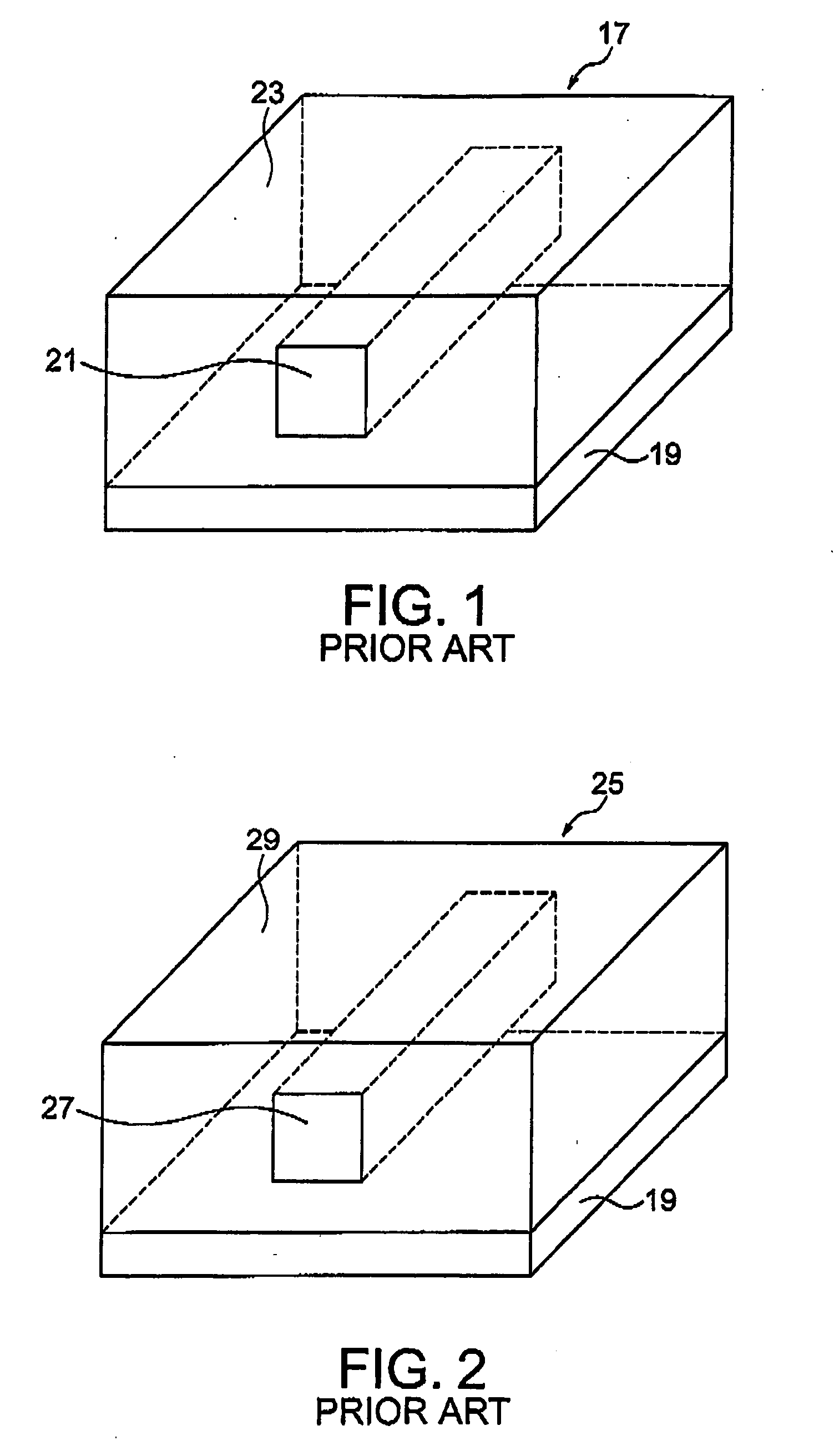
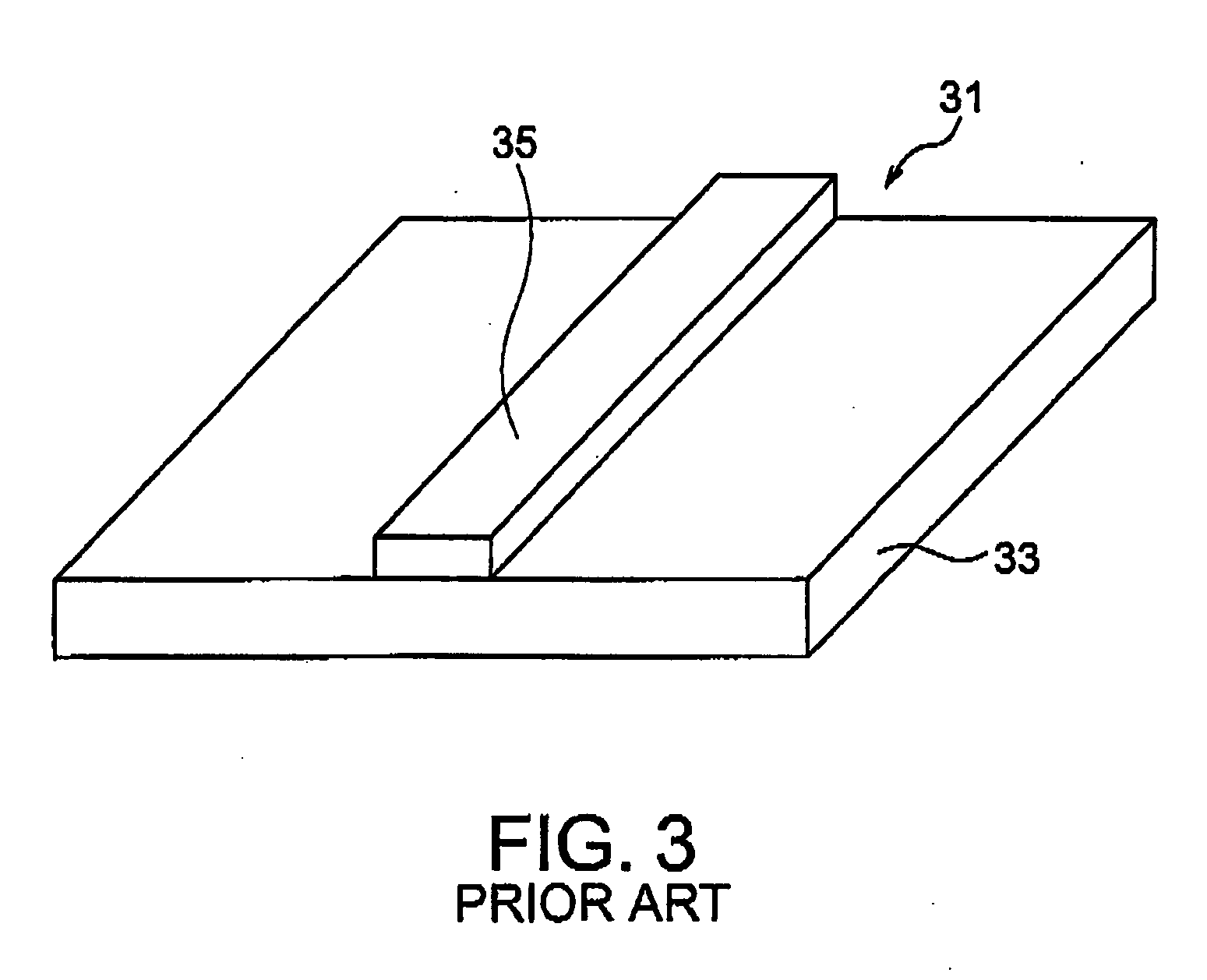
[0039] For a better understanding of the present invention, waveguides according to the related art will be explained using FIGS. 1 to 3 before explaining the embodiments of the present invention.
[0040] With reference to FIG. 1, a silica-based waveguide 17 of (i) has a core 21 and a cladding layer 23 made of silica glass (SiO2) formed on a substrate 19. By doping the core 21 with Ge or the like, a difference is made in refractive index between the core 21 and the cladding layer 23 of about 2 to 5% in order to guide light. It is widely used for a planer lightwave circuit (PLC). An AWG, which is used widely for communications, is achieved using this technique.
[0041] With reference to FIG. 2, a polymer-based waveguide 25 in (ii) has a core 27 and a cladding layer 29, both made of a polymer material such as PMMA or polyimide: a minute difference is made in refractive index between the material forming the core 27 and the material forming the cladding layer 29 in order to guide light. ...
PUM
 Abstract
Description
Claims
Application Information