Atomic layer deposition reactor

a technology of atomic layer and reactor, which is applied in the direction of chemical vapor deposition coating, metal material coating process, coating, etc., can solve the problems of contaminating the film, affecting the film quality, and exhibiting such ideal or near ideal behavior of precursors

Inactive Publication Date: 2005-05-05
KILPELA OLLI +6
View PDF58 Cites 413 Cited by
  • Summary
  • Abstract
  • Description
  • Claims
  • Application Information

AI Technical Summary

Benefits of technology

[0016] Another aspect of the present invention is a reactor configured to subject a substrate to alternately repeated surface reactions of vapor-phase reactants. The reactor includes a reaction chamber that defines a reaction space, the reaction space comprising a first section and a second section that are secured to each other through mechanical forces. A showerhead plate is disposed within the reaction space and divides the reaction space into a first part in which the substrate

Problems solved by technology

Cycles can also be more complex.
However, only a few precursors exhibit such ideal or near ideal behavior.
However, this method can result in sputtering by the plasma, which may contaminate the film as sputtered materials from parts in the reaction chamber contact the substrate.
Yet another disadvantage is that, when depositing conducting materials, arcing in the chamber can occur because the insulators used to

Method used


Image

  • Atomic layer deposition reactor
  • Atomic layer deposition reactor
  • Atomic layer deposition reactor

Examples


Embodiment Construction

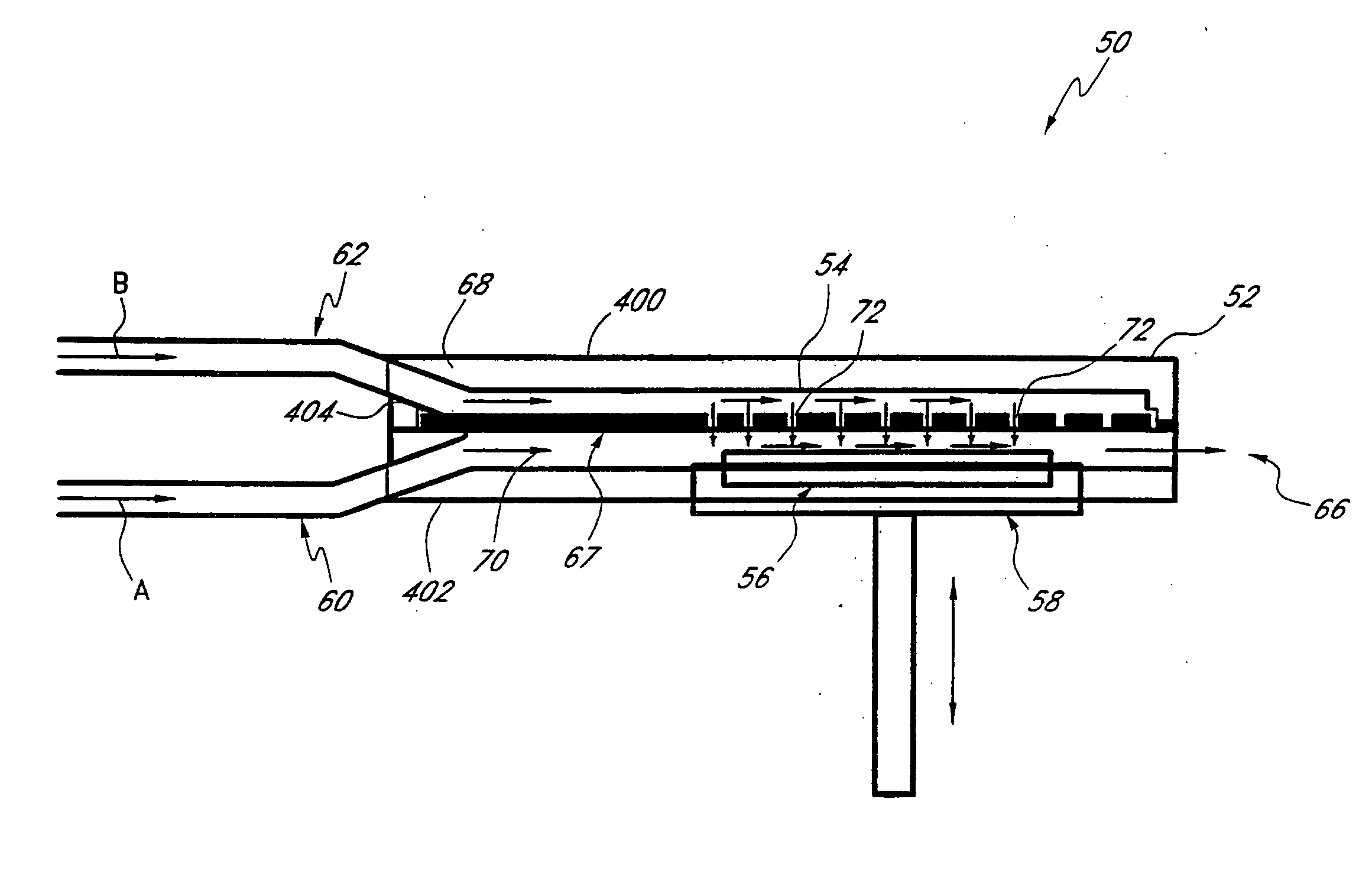
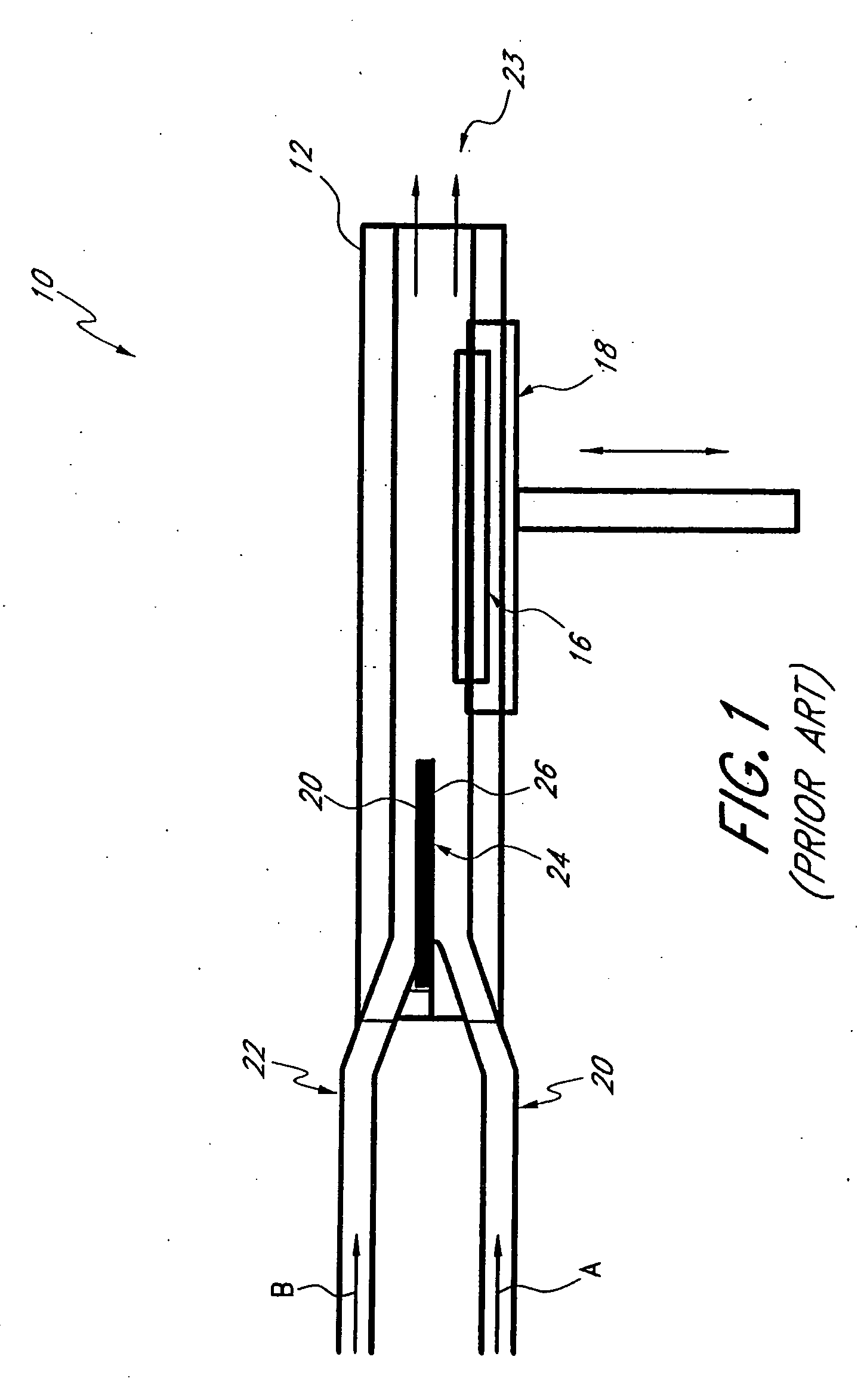
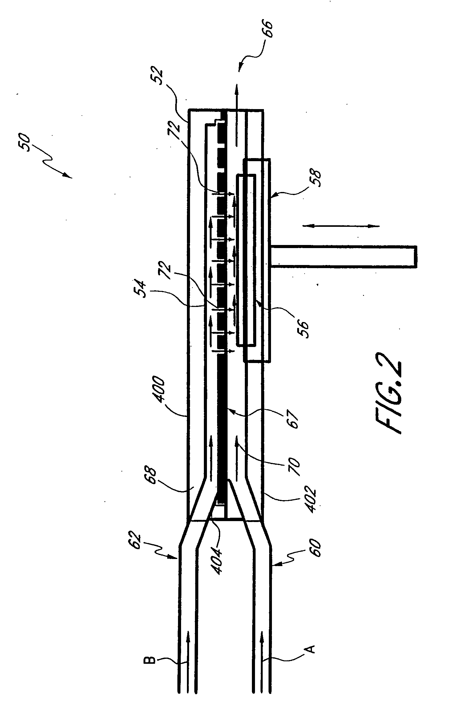
[0035]FIG. 1 schematically illustrates an exemplary prior art ALD reactor 10. The reactor 10 includes a reactor chamber 12, which defines, at least in part, a reaction space 14. A wafer or substrate 16 is disposed within the reaction chamber 14 and is supported by a pedestal 18. The pedestal 18 is configured to move the wafer 16 in and out of the reaction chamber 14. In other arrangements, the reactor can include an inlet / outlet port and an external robot with a robotic arm. The robot arm can be configured to (i) move the substrate into the reactor through the inlet / outlet port, (ii) place the substrate on the pedestal, (iii) lift the substrate from the pedestal and / or (iv) remove the substrate from the reactor through the inlet / outlet port.

[0036] In the illustrated reactor 10, two precursors, A and B, are supplied to the reaction space 14. The first precursor A is supplied to the reaction chamber 14 through a first supply conduit 20. In a similar manner, the second precursor B is ...


PUM

PropertyMeasurementUnit
Thicknessaaaaaaaaaa
Flow rateaaaaaaaaaa
Plasma poweraaaaaaaaaa

Abstract

Various reactors for growing thin films on a substrate by subjecting the substrate to alternately repeated surface reactions of vapor-phase reactants are disclosed. In one embodiment, the reactor comprises a reaction chamber. A showerhead plate divides the reaction chamber into upper and lower parts. A first precursor is directed towards the lower half of the reaction chamber and a second precursor is directed towards the upper half of the reaction chamber. The substrate is disposed within the lower half of the reaction chamber. The showerhead plate includes plurality passages such that the upper half is in communication with the lower half of the reaction chamber. In another arrangement, the upper half of the reaction chamber defines a plasma cavity in which in-situ radicals are formed. In yet another arrangement, the reaction chamber includes a shutter plate, which is configured to selectively open and close the passages in the showerhead plate. In other arrangements, the showerhead plate is arranged to modify the local flow patterns of the gases flowing through the reaction chamber.

Description

RELATED APPLICATION [0001] This application claims the priority benefit under 35 U.S.C. § 119(e) of U.S. Provisional Application No. 60 / 312,628 filed Aug. 15, 2001.BACKGROUND OF THE INVENTION [0002] 1. Field of the Invention [0003] The present invention relates to an apparatus for growing thin films on a surface of a substrate. More particularly, the present invention relates to an apparatus for producing thin films on the surface of a substrate by subjecting the substrate to alternately repeated surface reactions of vapor-phase reactants. [0004] 2. Description of the Related Art [0005] There are several methods for growing thin films on the surface of substrates. These methods include vacuum evaporation deposition, Molecular Beam Epitaxy (MBE), different variants of Chemical Vapor Deposition (CVD) (including low-pressure and organometallic CVD and plasma-enhanced CVD), and Atomic Layer Epitaxy (ALE), which was studied extensively for semiconductor deposition and electroluminescent ...

Claims


Application Information

Patent Timeline
IPC IPC(8): C23C16/44C23C16/452C23C16/455C23C16/507C23C16/509
CPCC23C16/4412C23C16/452C23C16/45514C23C16/45536C23C16/509C23C16/45565C23C16/45589C23C16/507C23C16/45544C23C16/00
Inventor KILPELA, OLLISAANILA, VILLELI, WEI-MINELERS, KAI-ERIKKOSTAMO, JUHANARAAIJMAKERS, IVOGRANNEMAN, ERNST
Owner KILPELA OLLI
Why Eureka
Try Eureka