Self-compensating antennas for substrates having differing dielectric constant values

Active Publication Date: 2005-05-05
AVERY DENNISON CORP
View PDF40 Cites 75 Cited by
  • Summary
  • Abstract
  • Description
  • Claims
  • Application Information

AI Technical Summary

Problems solved by technology

However, there are some practical constraints on what designs can be used with RFID tags and labels.
Nevertheless, even given the above, it is difficult to determine what is a ‘good’ antenna other than to require that it is one that does what you want, where you want and is built how you want it to be.
A low efficiency antenna, with a large loss resistance and relatively small radiation resistance, will not work well in most situations, as the majority of any power put into it will simply appear as heat and not as useful electromagnetic waves.
The problem is bandwidth, frequently described using the term Q (originally Quality Factor).
In addition, high Q/narrow band matching solutions are unstable, in that very small variations in component values or designs will cause large changes in performance.
However, sometimes it is not so simple to meet operational demands for the tag due to environmental or manufacturing constraints, and then other ways of achieving a good match must be considered.
These components do not normally include resistors, as these dissipate energy, which will generally lead to lower performance.
Now however, stuck to a block of higher dielectric constant material, the antenna is no longer operating in a medium having a dielectric c

Method used


Image

  • Self-compensating antennas for substrates having differing dielectric constant values
  • Self-compensating antennas for substrates having differing dielectric constant values
  • Self-compensating antennas for substrates having differing dielectric constant values

Examples


Embodiment Construction

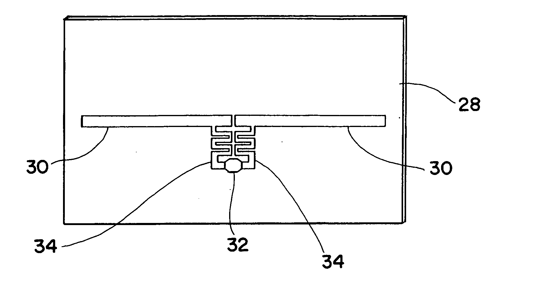
[0051] From the above it has been established that, if each tag could be tuned individually, using variable capacitors and inductors, or by changing the arm length, the tag could be made to work on any block of material having a dielectric constant. That cannot be done practically, but if the value and nature of the capacitors and inductors in the matching network are printed next to the antenna, and the elements that adjust the length of the arms, are a function of the substrate dielectric constant itself, with proper design, the tag could then adjust itself.

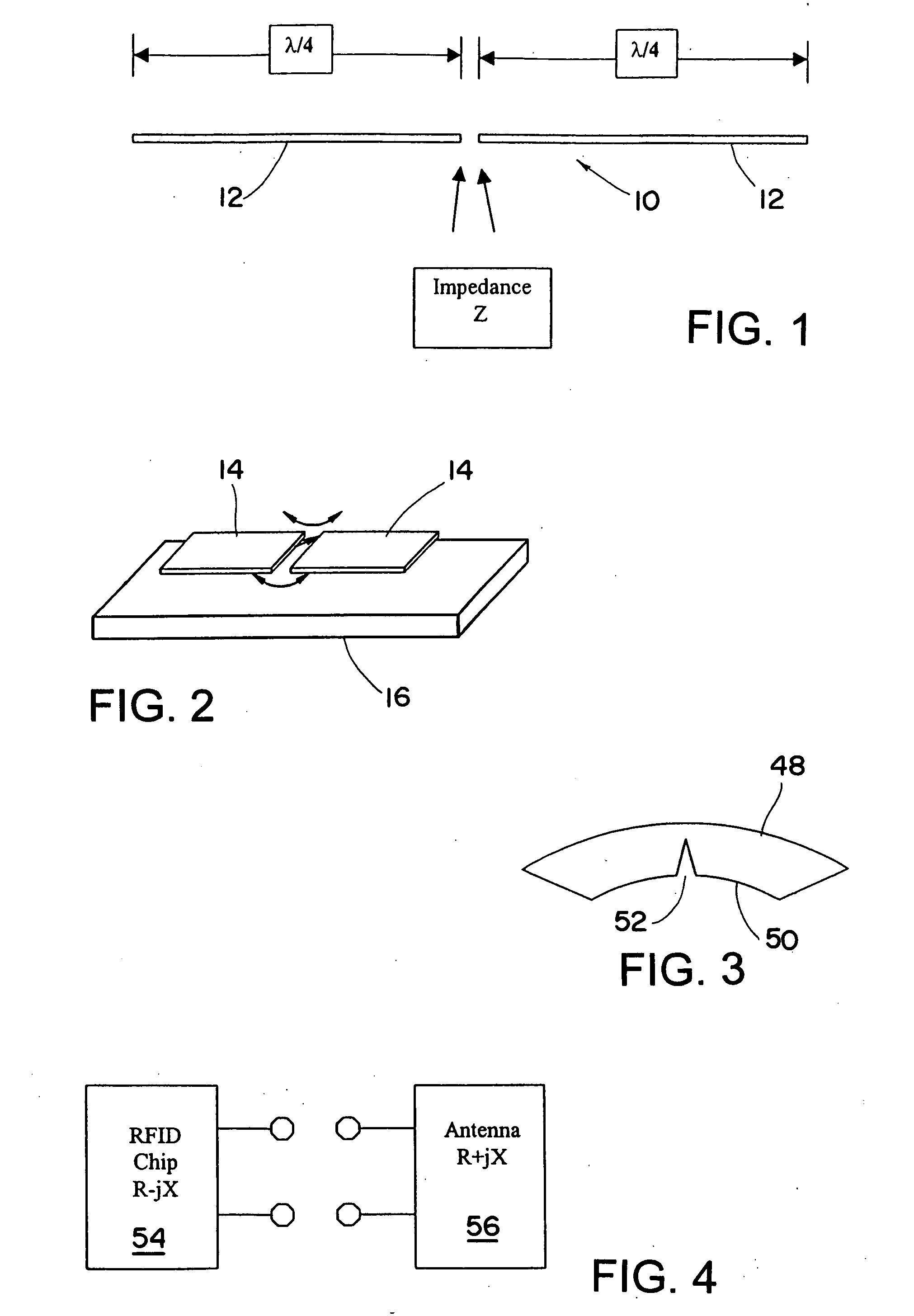
[0052] To illustrate further the concepts and preferred embodiments of the present invention, consider as an illustrative example, a simple half wave dipole antenna 10 as shown in FIG. 1. In free space, in its simplest form, the antenna will operate efficiently at the frequency where the two elements 12 are of equal length and are a quarter of a wavelength in the medium in which it is placed. The impedance Z of such an antenna...


PUM


Abstract

An RFID tag or label in combination with a dielectric material comprises a dielectric material and a wireless communication system that is mounted in electrical proximity to the dielectric material. The wireless communication system comprises a wireless communication device associated with an antenna system that has at least one conductive tab, including one or both of the following: (a) a plurality of electrical components that are selected to form an impedance matching network, that are coupled to the conducting tab and wireless communication device. The electrical components electrically interact with the dielectric material to maintain a substantial impedance match between the antenna system and the wireless communication device; and, (b) a structural element forming a frequency selective by-pass trap circuit formed in the conducting tab and electrically interacting with the dielectric material to maintain a substantial impedance match between the antenna system and the wireless communication device. The antenna system may be directly mounted on a dielectric substrate, which serves as the dielectric material Alternatively, the antenna system may be mounted on a backing layer intermediate the dielectric substrate and the antenna system, the backing layer in turn being attached to the dielectric substrate, wherein the backing layer and the dielectric substrate collectively serve as the dielectric material.

Description

BACKGROUND OF THE INVENTION [0001] 1. Field of the Invention [0002] This invention relates generally to the field of Radio Frequency Identification (RFID) tags and labels, and, in particular, to Radio Frequency Identification (RFID) tags and labels that include a self-compensating antenna structure that self-compensates for the material to which it is attached to maintain a substantial impedance match with such material so as to allow efficient performance of the tag. [0003] 2. Description of the Prior Art [0004] There is no simple definition of what constitutes an antenna, as all dielectric and conductive objects interact with electromagnetic fields (radio waves). What are generally called antennas are simply shapes and sizes that generate a voltage at convenient impedance for connection to circuits and devices. Almost anything can act to some degree as an antenna. However, there are some practical constraints on what designs can be used with RFID tags and labels. [0005] First, rec...

Claims


Application Information

Patent Timeline
IPC IPC(8): G06K19/077H01Q1/22H01Q9/28
CPCG06K19/07749H01Q9/285H01Q1/2225H01Q1/22
Inventor FORSTER, IAN J.
Owner AVERY DENNISON CORP
Why Eureka
Try Eureka