Dual-gate device and method

a technology of dual gate electrodes and semiconductors, applied in nanoinformatics, instruments, transistors, etc., can solve the problems of difference in threshold voltage, difficulty in using this current to determine difficulty in determining the actual threshold voltage of the device being read, so as to minimize the effect of charge disturbance and high density

Active Publication Date: 2008-04-10
SCHILTRON
View PDF11 Cites 9 Cited by
  • Summary
  • Abstract
  • Description
  • Claims
  • Application Information

AI Technical Summary

Benefits of technology

[0018]The present invention provides a non-volatile semiconductor memory device using a dual-gate structure that can b...

Problems solved by technology

Using this current to determine the actual threshold voltage of the device being read is difficult, as such a determination depends on being able to discriminate a current from a base current level that is affected by the programmed and erased states of all other memory cells in the string.
This method is made even more challenging by the small difference in threshold voltages between the programmed and the erased state of a device, due to the relatively great distance over which the stored electric charge must act to affect these threshold voltages.
The strong, uniform electrical interaction between the non-memory device and its associated memory device also results in read disturb in the memory cells in...

Method used


Image

  • Dual-gate device and method
  • Dual-gate device and method
  • Dual-gate device and method

Examples


Embodiment Construction

[0045]The present invention provides a dual-gate semiconductor memory device that includes a semiconductor channel material layer having a “sensitivity parameter” (discussed below) that is less than a predetermined value (e.g., 0.8). The dual-gate semiconductor memory device is suitable for use in three-dimensionally stacked memory circuits to achieve high circuit density. Additionally, when used in a NAND-type non-volatile semiconductor memory device, a memory device of the present invention experiences only minor disturbs of stored electric charge during programming and reading.

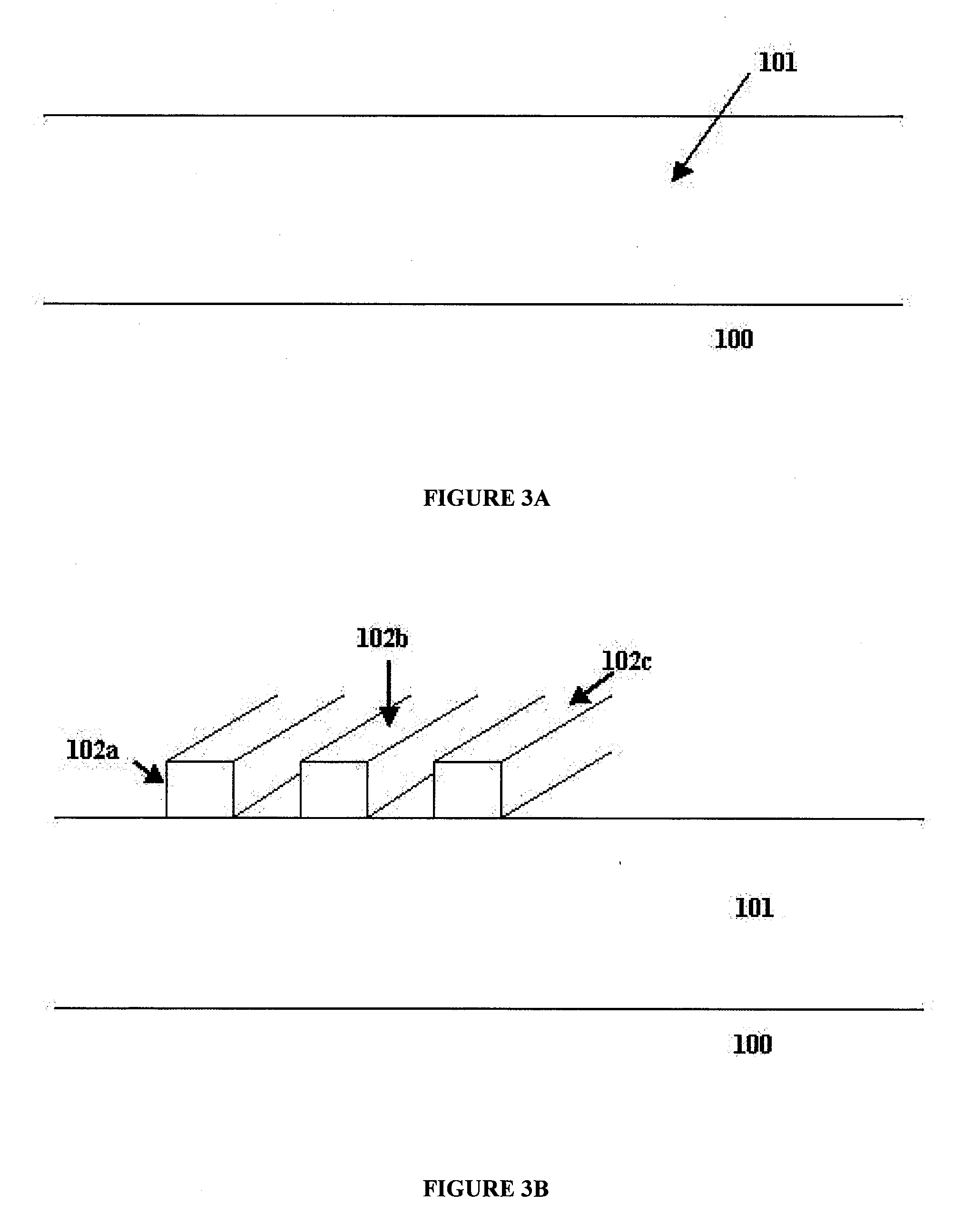
[0046]FIGS. 3A-3L illustrate a method suitable for forming a NAND-type non-volatile semiconductor memory device, according to one embodiment of the present invention.

[0047]FIG. 3A shows insulating layer 101 provided on substrate 100. Substrate 100 may be a semiconductor wafer containing integrated circuitry for controlling a non-volatile memory. The semiconductor wafer may be either of a bulk type, where th...


PUM


Abstract

A memory circuit having dual-gate memory cells and a method for fabricating such a memory circuit are disclosed. The dual-gate memory cells each include a memory device and an access device sharing a semiconductor layer, with their respective channel regions provided on different surfaces of the semiconductor layer. The semiconductor layer has a thickness such that a sensitivity parameter relating an electrical interaction between the gate electrodes of the access device and the memory device is less than a predetermined value. The dual-gate memory cells can be used as building blocks for a non-volatile memory array, such as a memory array formed by NAND-strings. In such an array, during programming of a nearby memory device in a NAND string, in NAND-strings not to be programmed, if inversion regions are allowed to be formed in the semiconductor layer, or if the semiconductor layer is allowed to electrically float, electrical interaction exists between the access devices and the memory devices to inhibit programming of the memory devices.

Description

CROSS-REFERENCE TO RELATED APPLICATIONS [0001]The subject matter of the present patent application is related to (a) U.S. patent application Ser. No. 11 / 000,114 (“the '114 application”), entitled “Dual-Gate Device and Method,” filed on Nov. 29, 2004 and to U.S. patent application Ser. No. 11 / 197,462 (“the '462 application”), entitled “Dual-Gate Device and Method,” filed on Aug. 3, 2005. Disclosures of the '114 and '462 applications are hereby incorporated by reference in their entireties.BACKGROUND OF THE INVENTION [0002]1. Field of the Invention[0003]The present invention relates to a semiconductor device. In particular, it relates to a semiconductor device having dual gate electrodes.[0004]2. Discussion of the Related Art[0005]Dual-gate semiconductor devices have been used as non-volatile memory devices. For example, K. Yanagidaira et al (“Yanagidaira's paper”), IEEE Electron Device Letters, vol. 26, pp. 473-475, July 2005, report a dual-gate silicon nanocrystal memory where elect...

Claims


Application Information

Patent Timeline
IPC IPC(8): H01L29/788G11C11/34H01L21/336
CPCG11C16/10H01L21/28273H01L21/28282H01L27/115H01L29/792H01L27/11568H01L29/4234H01L29/42352H01L27/11521H01L29/40114H01L29/40117H10B43/30H10B69/00H10B41/30H01L29/788H01L27/105B82Y10/00
Inventor WALKER, ANDREW J.
Owner SCHILTRON
Why Eureka
Try Eureka