Semiconductor package, method for manufacturing the same and lead frame for use in the same

Active Publication Date: 2005-05-05
ADVANCED SEMICON ENG INC
View PDF36 Cites 19 Cited by
  • Summary
  • Abstract
  • Description
  • Claims
  • Application Information

AI Technical Summary

Benefits of technology

[0008] The object of the present invention is to provide a semiconductor package that efficiently increases the fillet height without inverse effect on the

Problems solved by technology

However, as ICs products are endlessly speeded and shrank, the conventional lead frame package has become unfashionable, at least for some efficiency-concerned ICs products.
However, for small I/Os the lead frame package still occupies the quite large market share, because it provides the solutions of the low cost efficiency.
Because of having quite long inner leads and out

Method used


Image

  • Semiconductor package, method for manufacturing the same and lead frame for use in the same
  • Semiconductor package, method for manufacturing the same and lead frame for use in the same
  • Semiconductor package, method for manufacturing the same and lead frame for use in the same

Examples


Example

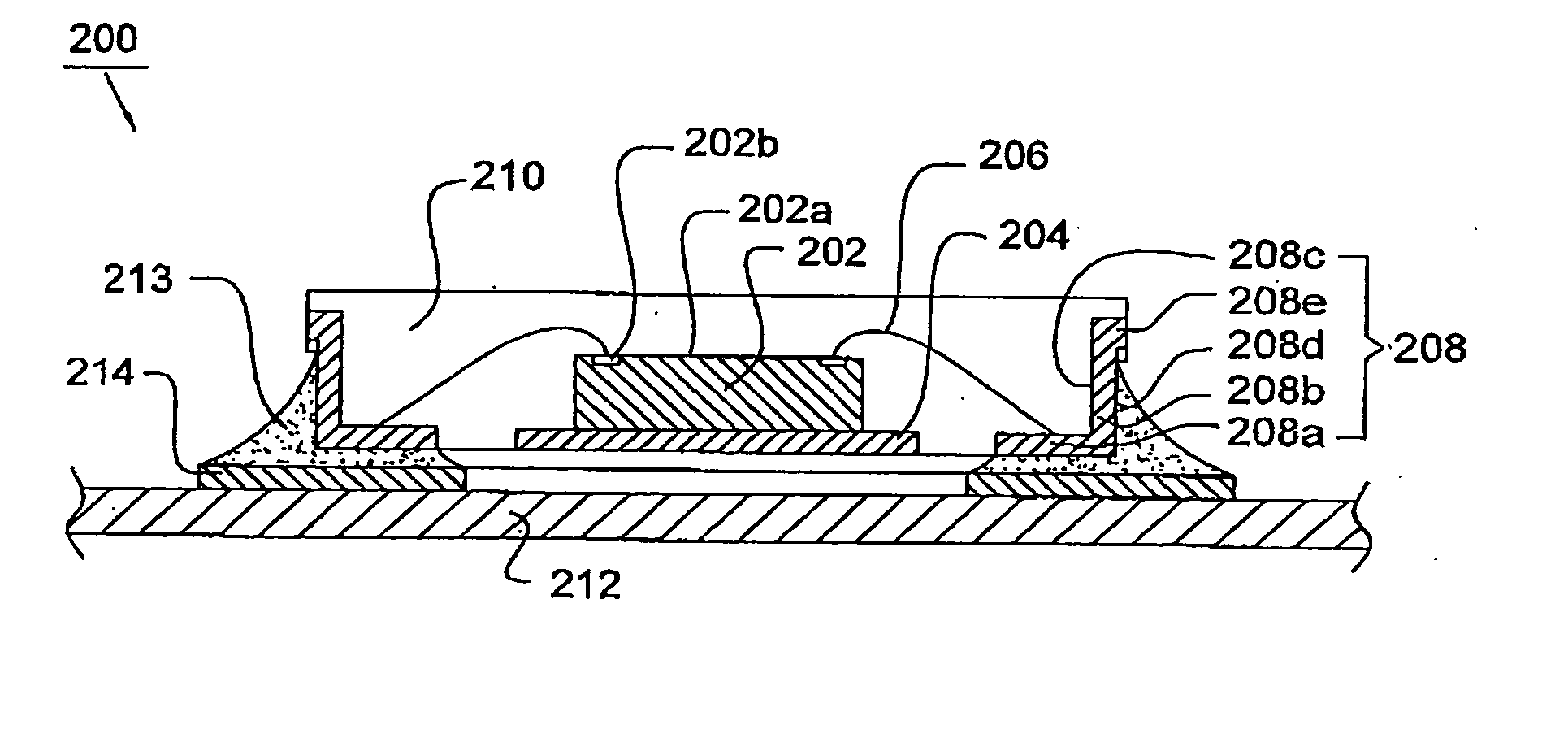
[0019]FIG. 2 discloses a semiconductor package 200 of one embodiment in accordance with the present invention. It comprises a semiconductor chip 202 that is attached to a die pad 204 by a conductive resin or non-conductive resin, for example, epoxy resin (not shown in the figure). The active area 202a of the semiconductor chip 202 has a plurality of bonding pads 202b. A plurality of leads 208 are placed in the periphery of the semiconductor chip 202. Each of the leads 208 has a first portion 208a, a second portion 208b that curves upwards and opposing upper surface 208c and lower surface 208d. A plurality of bonding wires 206 each having one end connected to the first portion 208a of the L-shaped lead 208 and the other end connected to the bonding pad 202b of the semiconductor chip 202. The second portion 208b of the lead 208 may comprise a protrusion 208e. A package body 210 encloses the semiconductor chip 202 and leads 208, wherein the whole lead 208 is substantially embedded in t...


PUM


Abstract

A semiconductor package mainly includes a semiconductor chip and a plurality of leads at the periphery of the semiconductor chip. Each of the leads has a first portion, a second portion and opposing upper and lower surfaces, wherein the second portion of the leads are bent upwards. The semiconductor package has a plurality of bonding wires with one ends connected to the bonding pads of the semiconductor chip and the other ends connected to the first portions of the leads. The semiconductor package is provided with a package body formed over the semiconductor chip and the leads, wherein each of the leads is substantially embedded in the package body with the lower surface thereof exposed from the package body. The present invention further provides a method for manufacturing the semiconductor package.

Description

[0001] This application claims the priority benefit of Taiwan Patent Application Serial Number 092130070 filed Oct. 29, 2003, the full disclosure of which is incorporated herein by reference. FIELD OF THE INVENTION [0002] The present invention relates to a lead frame package. BACKGROUND OF THE INVENTION [0003] Because of low price and high reliability, a lead frame package has been used in the field of the ICs package for a long time. However, as ICs products are endlessly speeded and shrank, the conventional lead frame package has become unfashionable, at least for some efficiency-concerned ICs products. Therefore, the ball grid array (BGA) and chip scale package (CSP) have become a new choice for package. The BGA is widely applied to chips with large I / Os and chips that need better electronic properties and heat efficiency (for example, central processing unit and graphic chips). The CSP has also been wildly used in portable products, having main concerns for footprints, package p...

Claims


Application Information

Patent Timeline
IPC IPC(8): H01L23/495H01L25/10H05K3/34
CPCH01L23/49551H01L25/105H01L2224/16H01L2224/48091H01L24/48H01L2924/30107H05K3/3442H01L2224/48247H01L2924/00014H01L2924/181H01L2924/00012H01L2224/45099H01L2224/45015H01L2924/207
Inventor LIU, SHENG TSUNG
Owner ADVANCED SEMICON ENG INC
Why Eureka
Try Eureka