PLL clock signal generation circuit

a clock signal and phaselocked loop technology, applied in the direction of oscillator tubes, pulse automatic control, electrical equipment, etc., can solve the problem of increasing the load on the cpu, and achieve the effect of stable action performan

Inactive Publication Date: 2005-05-12
III HLDG 12 LLC
View PDF10 Cites 21 Cited by
  • Summary
  • Abstract
  • Description
  • Claims
  • Application Information

AI Technical Summary

Benefits of technology

[0020] Therefore, according to the first characteristics of the PLL clock signal generation circuit mentioned above, the reference to the reference voltage which is an output of the filter circuit enables the detection of a state of locking of the PLL clock signal generation circuit, and also enables the change of multiple rate of the divider prior to the transition of the reference voltage to a state corresponding to a saturation of the voltage control oscillator, thereby adjusting a reference voltage to be capable of maintaining a state of locking of the PLL clock signal generation circuit. In this way, a PLL clock signal generation circuit is achieved that can maintain a proper state of locking even in the case when the operation region of the voltage control oscillator is narrow.
[0021] Additionally in the second characteristics, the PLL clock signal generation circuit according to the first characteristics of the present invention preferably includes a first Schmitt trigger circuit capable of detecting the multiple rate control circuit having the reference voltage higher than the upper limit value of the voltage range capable of locking, a second Schmitt trigger circuit capable of detecting the reference voltage lower than the lower limit value of the voltage range capable of locking, a D flip-flop determining that the reference voltage being higher than the upper limit value and outputting the control signal for increasing a ratio of division of the divider when the both the first Schmitt trigger circuit and the second Schmitt trigger circuit show the high level output state, and a control circuit determining that the reference voltage being lower than the lower limit value and resetting the D flip-flop when the both the first Schmitt trigger circuit and the second Schmitt trigger circuit show the low level output state. Such configuration of the multiple rate control circuit allows a proper and a stable detection of a state of the reference voltage and delivers a stable performance of the action and an effect of the first characteristics mentioned above.
[0022] Furthermore in the third characteristics, the PLL clock signal generation circuit according to the second characteristics of the present invention preferably has each of the hysteresis width of the first Schmitt trigger circuit and the second Schmitt trigger circuit set to a value above a ripple voltage overlapping the output voltage of the charge pump circuit. Such configuration of the Schmitt trigger circuit allows a safer design not susceptible to the ripple voltage of the charge pump circuit.

Problems solved by technology

This increases the load to the CPU.

Method used


Image

  • PLL clock signal generation circuit
  • PLL clock signal generation circuit
  • PLL clock signal generation circuit

Examples


Embodiment Construction

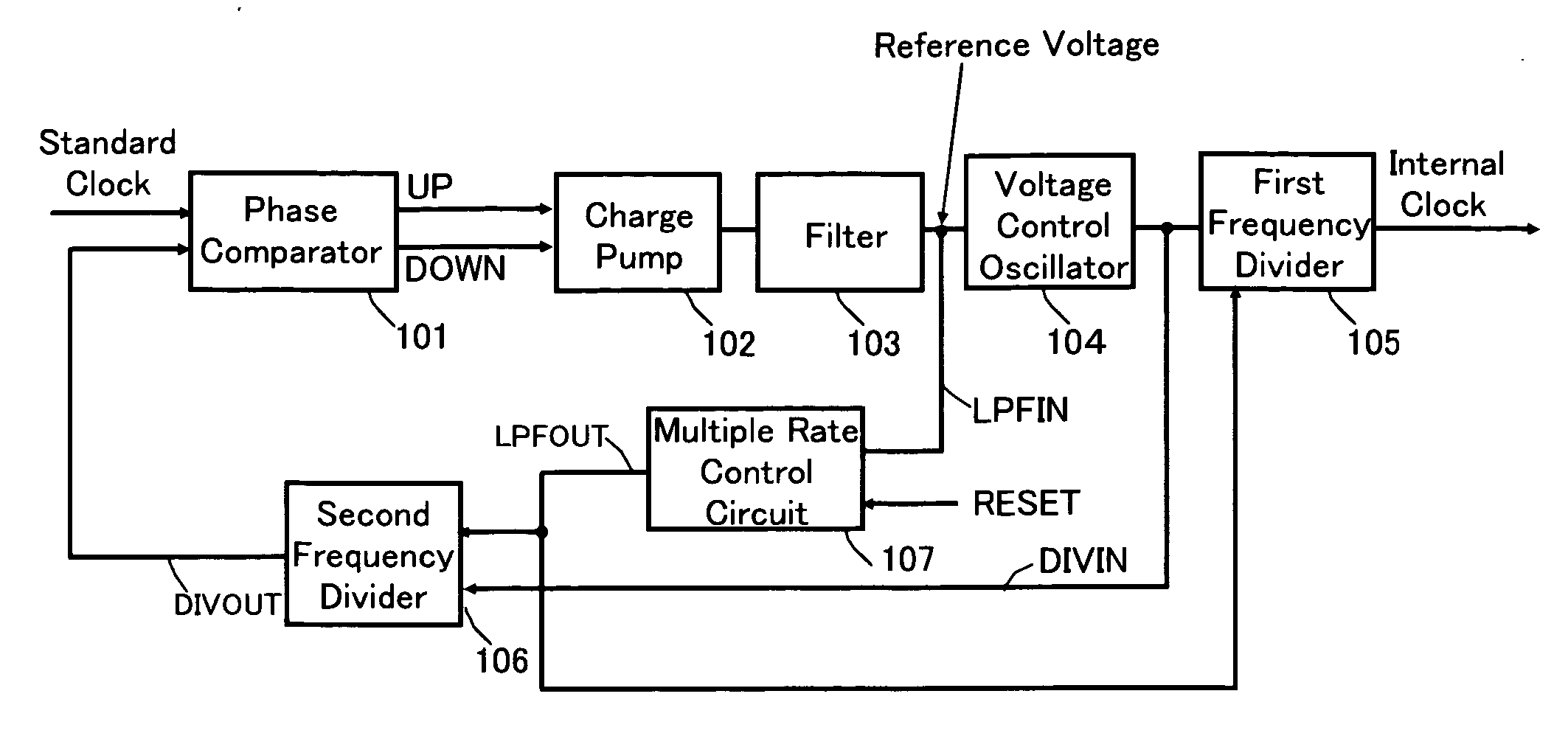
[0033] An embodiment of the PLL clock signal generation circuit according to the present invention (hereinafter, referred to as “the present circuit”) will be described with reference to the drawings. The same reference numerals are used to refer the same circuit components of the conventional PLL clock signal generation circuit throughout the various views.

[0034] As shown in FIG. 1, the present circuit includes a multiple rate control circuit 107 in addition to a phase comparator 101, a charge pump circuit 102, a filter circuit 103, a voltage control oscillator 104, a first frequency divider 105 and a second frequency divider 106. All circuits, but a multiple rate control circuit 107, are the same with the corresponding circuits of the conventional PLL clock signal generation circuit shown in FIG. 5. The multiple rate control circuit 107 is input by a reference voltage (name of the signal: LPFIN) which is an output of the filter circuit 103, and the output (name of the signal: LPF...


PUM


Abstract

A PLL clock signal generation circuit comprising a phase comparator, a charge pump circuit, a filter circuit, a voltage control oscillator and a divider, wherein a multiple rate control circuit is further included which detects a state of the reference voltage (output from a filter circuit) and controls a change of a multiple rate of a divider according to a state of the detected reference voltage. The multiple rate control circuit further outputs control signal LPFOUT for changing a multiple rate so that the PLL clock signal generation circuit does not deviate from a region capable of locking when being detected of deviation from the region capable of locking by detecting the state of reference voltage.

Description

CROSS REFERENCE TO RELATED APPLICATIONS [0001] This Nonprovisional application claims priority under 35 U.S.C. §119(a) on patent application Ser. No. JP2003-380153 filed in Japan on 10 Nov. 2003, the entire contents of which are hereby incorporated by reference. BACKGROUND OF THE INVENTION [0002] 1. Field of the Invention [0003] The present invention relates to a PLL (Phase-Locked Loop) clock signal generation circuit, and it particularly relates to technology for increasing stable operation region (lock range). [0004] 2. Description of the Related Art [0005] In the increasing demands for an IC card in the recent years, there has been a strong request for stable operations of an integrated PLL clock signal generation circuit even in a wide variation range of a standard clock input from outside the circuit, thus involving an increase of lock range of the PLL clock signal generation circuit. [0006]FIG. 5 shows configuration of a basic PLL clock signal generation circuit. The PLL clock...

Claims


Application Information

Patent Timeline
Patent Type & Authority Applications(United States)
IPC IPC(8): H03L7/089H03L7/095H03L7/10H03L7/197
CPCH03L7/0891Y10S331/02H03L7/197H03L7/10H03L7/103
Inventor SAKAMOTO, YASUHIKONAKAO, YOSHIHIRO
Owner III HLDG 12 LLC
Why Eureka
Try Eureka