Method for performing a burn-in test

a burn-in test and burn-in technology, applied in the field of integrated circuits, can solve the problems of generating false failures, significantly longer time, and exceeding the retention time specification of dram cells

Inactive Publication Date: 2005-05-12
QIMONDA +1
View PDF6 Cites 73 Cited by
  • Summary
  • Abstract
  • Description
  • Claims
  • Application Information

AI Technical Summary

Benefits of technology

[0004] A second aspect of the present invention is a DDR DRAM having a low frequency and a high frequency operating mode, comprising: a multiplicity of storage cells arranged in an array, each storage cell accessible by a wordline and a bitline; and wherein peripheral logic circuits of the DDR DRAM are adapted to execute a write burst enable and a column addre...

Problems solved by technology

Insitu burn-in testing of a DRAM in DDR mode, therefore, takes a significantly longer time than in SDR mode and can exceed the retention time...

Method used


Image

  • Method for performing a burn-in test
  • Method for performing a burn-in test
  • Method for performing a burn-in test

Examples


Embodiment Construction

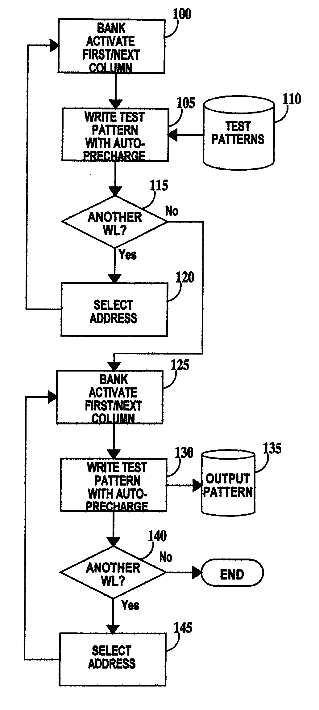
[0012] Cells in a DRAM are arranged in a two dimensional matrix, with rows being accessed by wordlines and columns being accessed by bitlines. A typical DRAM cell consists of an N channel field effect transistor (NFET) transistor and a storage node (usually a capacitor). The gate of the NFET is connected to a wordline, the drain to a bitline, the source to a first plate of the capacitor and the second plate of the capacitor is connected to a low voltage, usually to ground. Sense amplifiers on each bitline sense the presence of stored charge (a logical 1) on the storage node of a DRAM cell when that cells wordline is turned on.

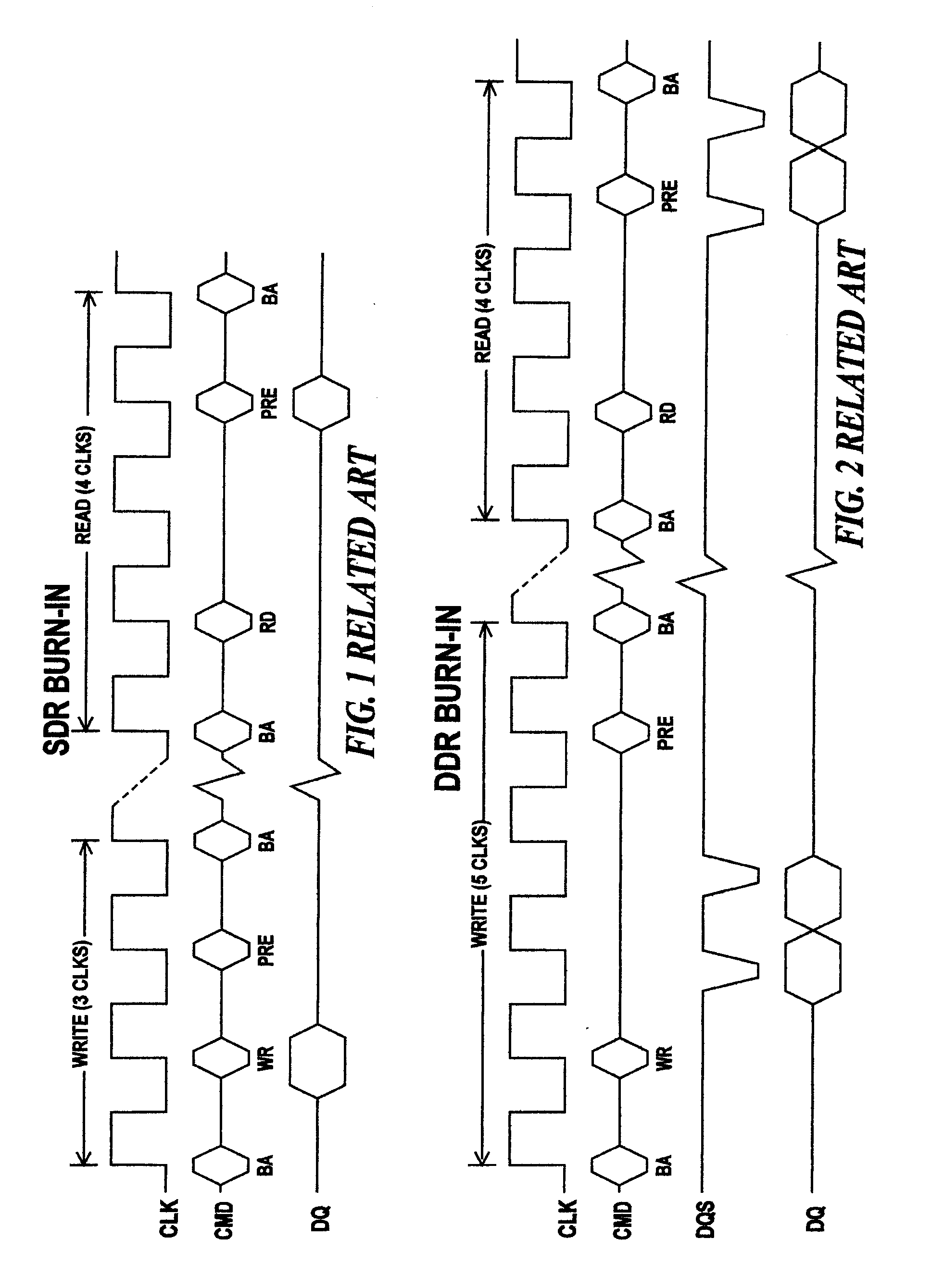
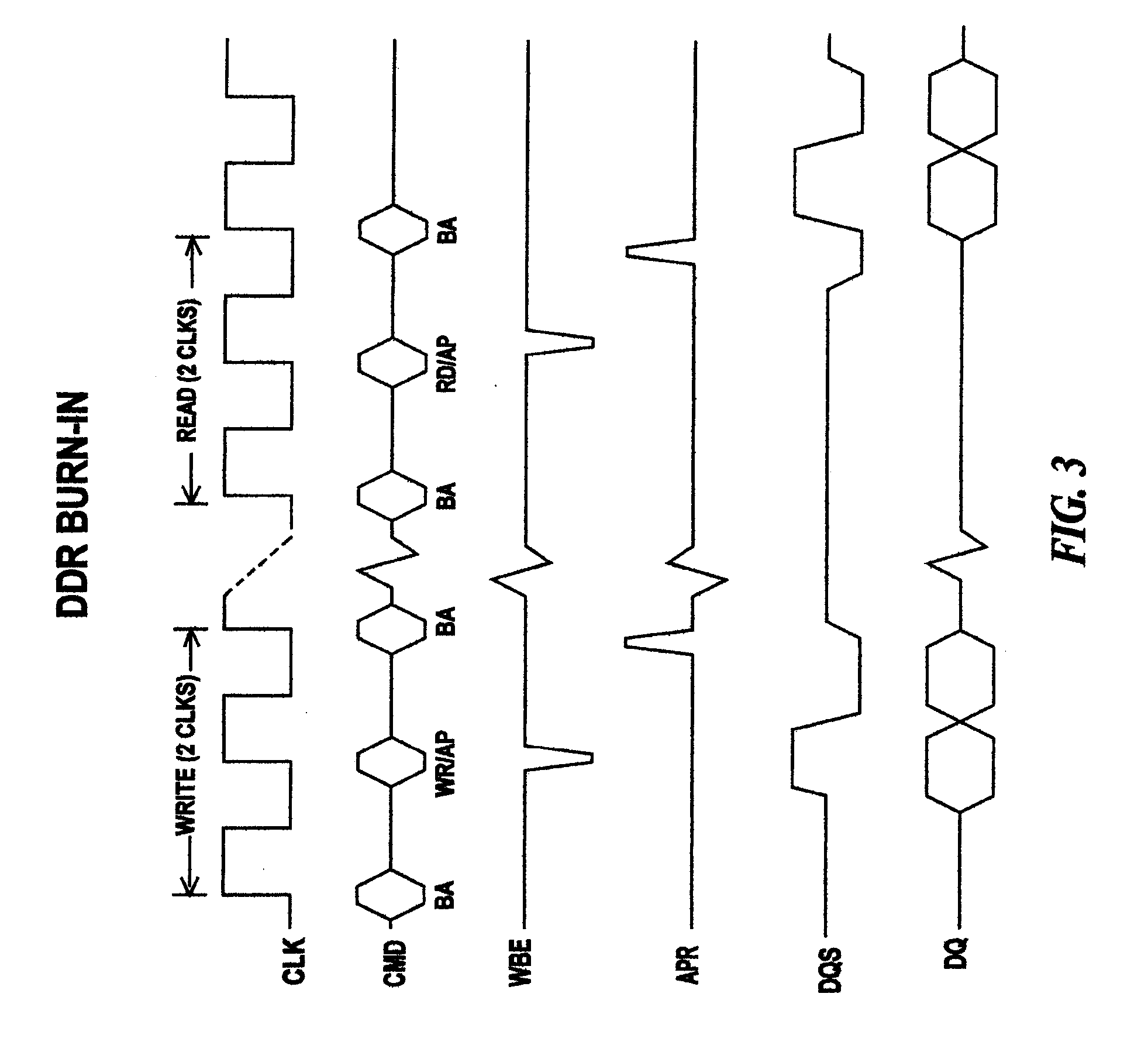
[0013] Operation of a DRAM in SDR / DDR mode is covered in the JEDEC Standards SDRAM3—11—05 / JESD97 specification. The circuit design to meet this specification varies from manufacturer to manufacturer.

[0014] Burn-in testing of DRAMs is designed to provide accelerated fail of cells during test that would otherwise fail subsequently. Acceleration is accomplished ...


PUM


Abstract

A method for testing a DDR DRAM having a test mode and an operational mode is described. The method including in the order recited: (a) placing the DDR DRAM in test mode; (b) issuing a bank activate command to select and bring up a wordline selected for write of the DDR DRAM; (c) writing with auto-precharge, a test pattern to cells of the DDR DRAM; (d) repeating steps (b) and (c) until all wordlines for write have been selected; (e) issuing a bank activate command to select and bring up a wordline selected for read of the DDR DRAM; (f) reading with auto-precharge, the stored test pattern from cells of the DDR DRAM; and (g) repeating steps (e) and (f) until all wordlines for read have been selected.

Description

BACKGROUND OF INVENTION [0001] The present invention relates to the field of integrated circuits; more specifically, it relates to double data rate (DDR) dynamic random access memory (DRAM) burn-in testing. [0002] Two main types of DRAMs are, single data rate (SDR) and a double data rate (DDR). In SDR mode, data comes out of the DRAM on a rising clock edge. In DDR mode, data is delivered externally on both a rising and falling clock edge. Furthermore, DDR architecture requires a two clock internal write latency (the number of clocks of delay from when the write command is issued to the DRAM externally until the column select is activated in the DRAM array), while SDR requires no internal write latency. Insitu burn-in testing of a DRAM in DDR mode, therefore, takes a significantly longer time than in SDR mode and can exceed the retention time specification of the DRAM cell, generating false fails. Current testing methods of dual mode (SDR and DDR) DRAMs therefore rely only on insitu ...

Claims


Application Information

Patent Timeline
IPC IPC(8): G11C29/00G11C29/08
CPCG11C11/401G11C2029/1202G11C29/08
Inventor NORRIS, ALAN D.WEINSTEIN, SAMUELWUENSCHE, STEPHAN
Owner QIMONDA
Why Eureka
Try Eureka