

Method and structure to use an etch resistant liner on transistor gate structure to achieve high device performance
a transistor gate and etch resistant technology, applied in the direction of semiconductor devices, diodes, electrical devices, etc., can solve the problems of insufficient resistance of spacers, inability to resist etching, and inability to protect the sidewalls of gate stacks
- Summary
- Abstract
- Description
- Claims
- Application Information
AI Technical Summary
Benefits of technology
Problems solved by technology
Method used
Image

Examples
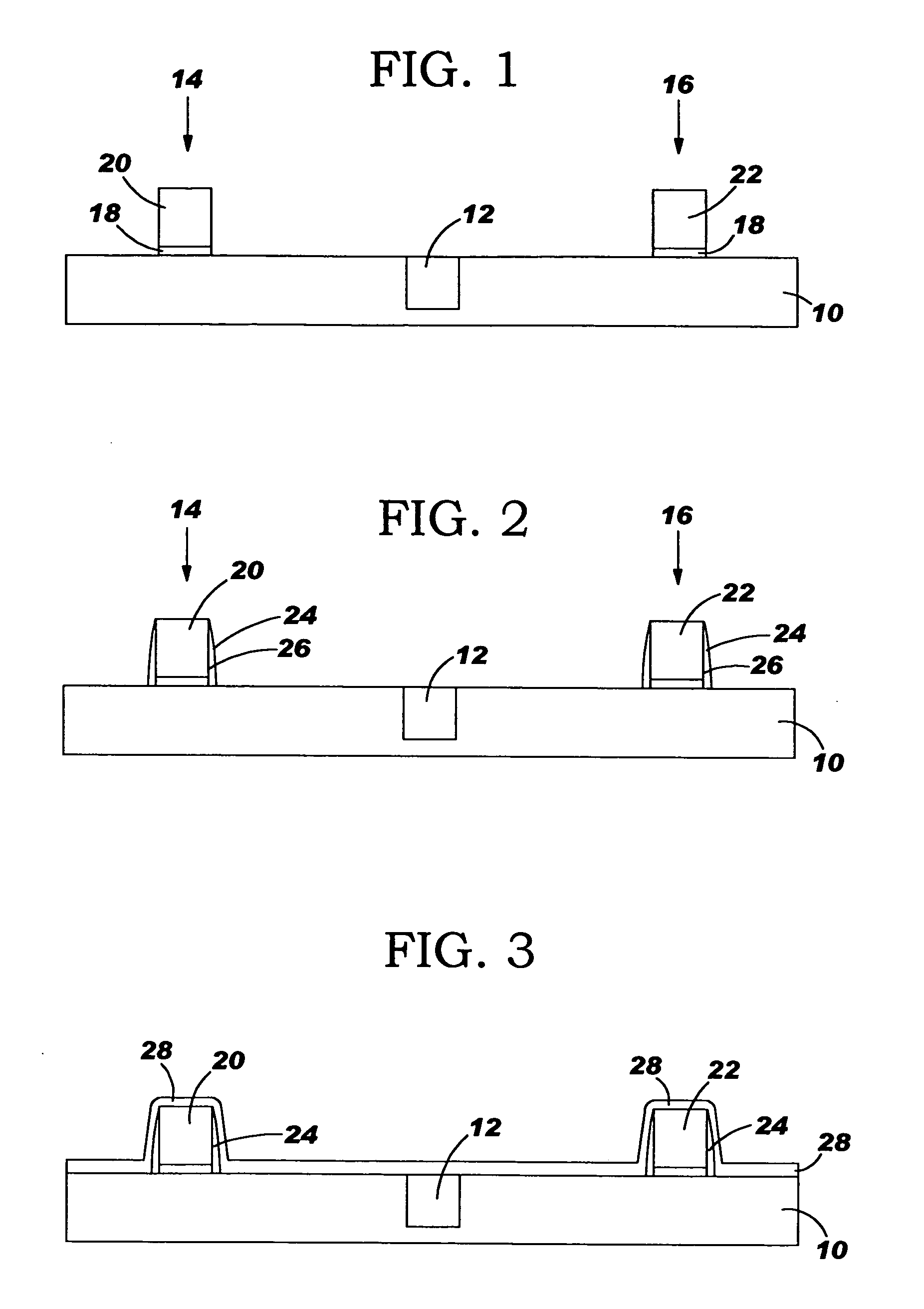
first embodiment
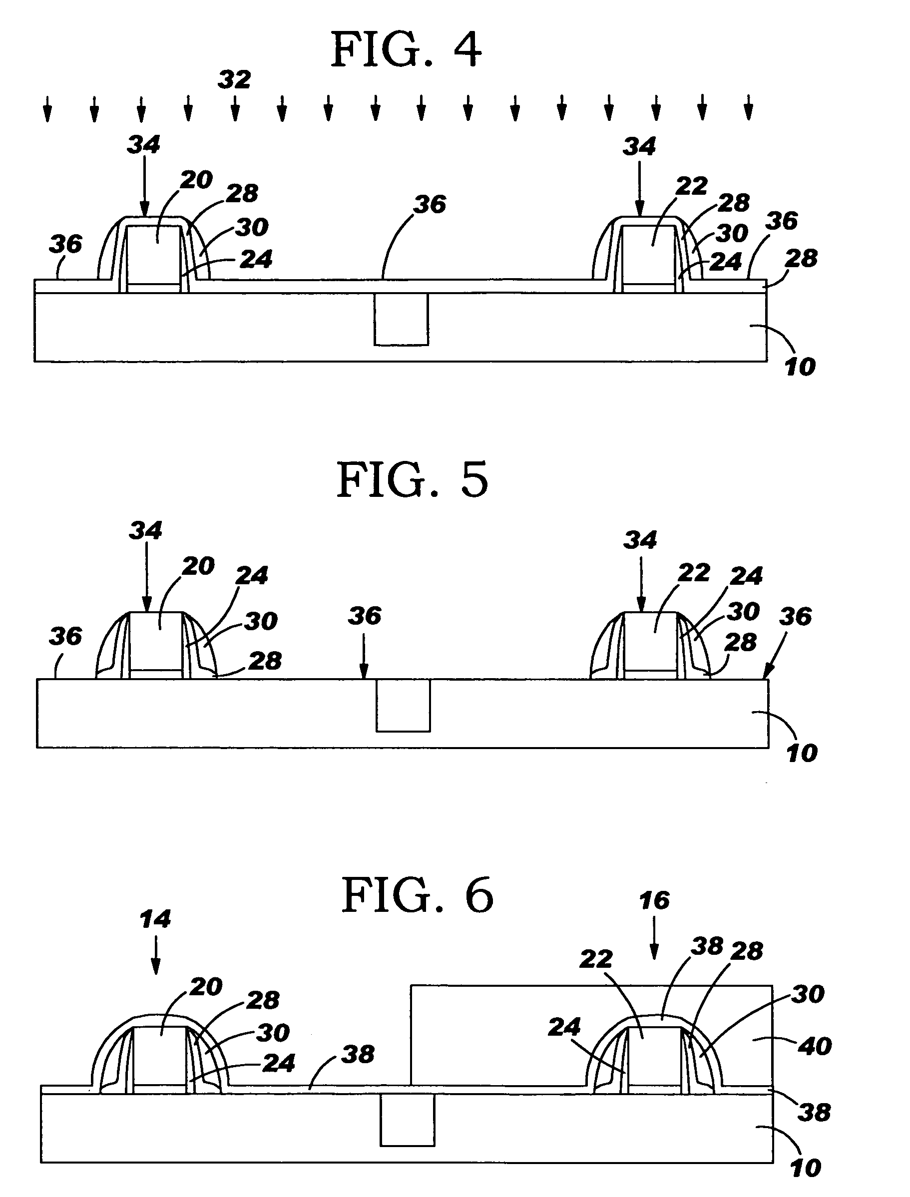
[0057] Thereafter, the wet etch is performed to remove the damaged portions of the liner 28 in regions 34 and 36, and the photoresist 54 is removed, as illustrated in FIG. 11. As described in connection with the first embodiment, the protective layer 38 is conformally deposited over the surface of the substrate 10 (FIG. 12). A photoresist 40 is then deposited, patterned and etched, using conventional processes, to cover the resistor region 16 of the substrate 10 and leave the transistor region 14 of the substrate 10 uncovered (FIG. 12). An etch process, such as a RIE, or other similar process, is performed to remove the protective layer 38 from the surface of the substrate 10 in the transistor region 14, as illustrated in FIG. 13. The remaining photoresist 40 is also removed leaving the protective layer 38 over the resistor region 16 of the substrate 10 (FIG. 13).
[0058] Thereafter, the preclean process is performed to prepare the surface of the substrate 10 in the transistor region ...
third embodiment
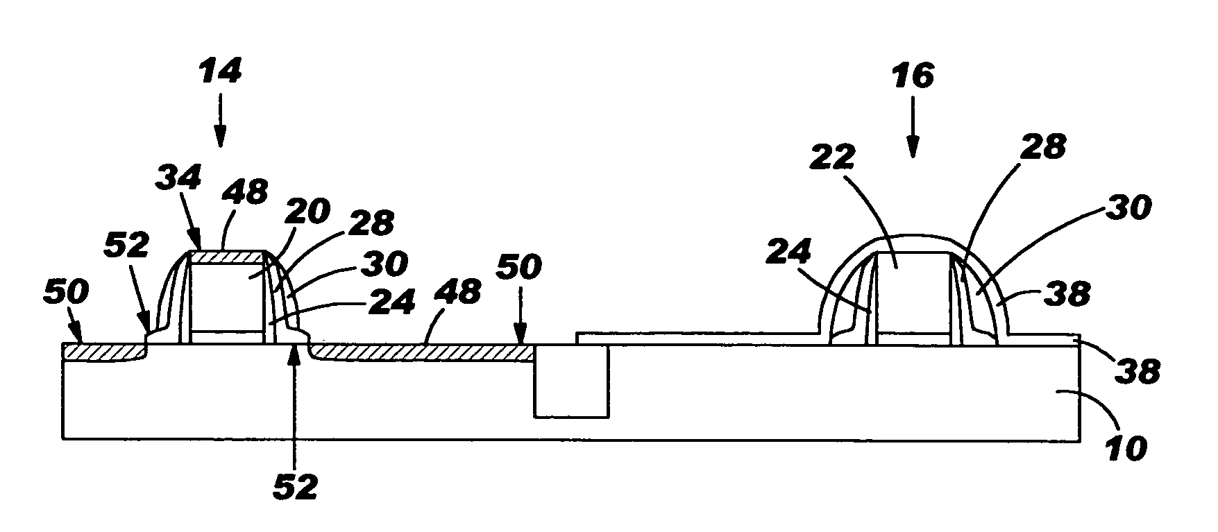
[0060] A third embodiment is illustrated in FIGS. 16-22. Instead of forming the first spacer 24 along the sidewalls 26 of the transistor gate stack 20 and the resistor gate stack 22, the liner 28 is formed directly on the gate stacks 20, 22, as illustrated in FIG. 16. Thereafter, spacer 30 is formed on the liner 28 along the sidewalls 26 of the gate stacks 20, 22, as illustrated in FIG. 17.
[0061] Ions 32 may then be implanted into the surface of the substrate 10 to damage exposed regions of the liner 30, as illustrated in FIG. 17. As described in the first embodiment, the exposed regions of the liner 28 are intentionally damaged by the ion implantation. The damaged portions of the liner 28 are then chemically removed using a wet etch, as illustrated in FIG. 18.
[0062] As illustrated in FIG. 19, layer 38 is conformally deposited over the surface of the substrate 10. A photoresist 40 is then deposited, patterned and etched, using conventional processes, to cover the resistor region 16...
PUM
 Abstract
Description
Claims
Application Information