Electrostatic chuck for supporting a substrate

a technology of electrostatic chuck and substrate, which is applied in the direction of emergency protective circuit arrangement, electrical equipment, emergency protective arrangement details, etc., can solve the problems of damage to the body and damage to the insulation layer formed on the inner face of the hole, and achieve the effect of preventing damage to the body

Inactive Publication Date: 2005-05-19
SAMSUNG ELECTRONICS CO LTD
View PDF18 Cites 47 Cited by
  • Summary
  • Abstract
  • Description
  • Claims
  • Application Information

AI Technical Summary

Benefits of technology

[0012] In general, exemplary embodiments of the present invention provide an electrostatic chuck for minimizing the generation of

Problems solved by technology

RF power or bias power applied to the body of the electrostatic chuck may cause damage to the insulation layer formed on the inne

Method used


Image

  • Electrostatic chuck for supporting a substrate
  • Electrostatic chuck for supporting a substrate
  • Electrostatic chuck for supporting a substrate

Examples


Embodiment Construction

[0025] The present invention now will be described more fully hereinafter with reference to the accompanying drawings, in which exemplary embodiments of the present invention are shown. This invention may, however, be embodied in many different forms and should not be construed as limited to the exemplary embodiments set forth herein, but it should be recognized that these exemplary embodiments are provided so that this disclosure will be thorough and complete, and will fully convey the scope of the invention to those skilled in the art. It should be understood that as used herein, when an element such as a layer, region or substrate is described as being “on” or deposited “onto” another element, such language does not preclude the presence of one or more intervening elements.

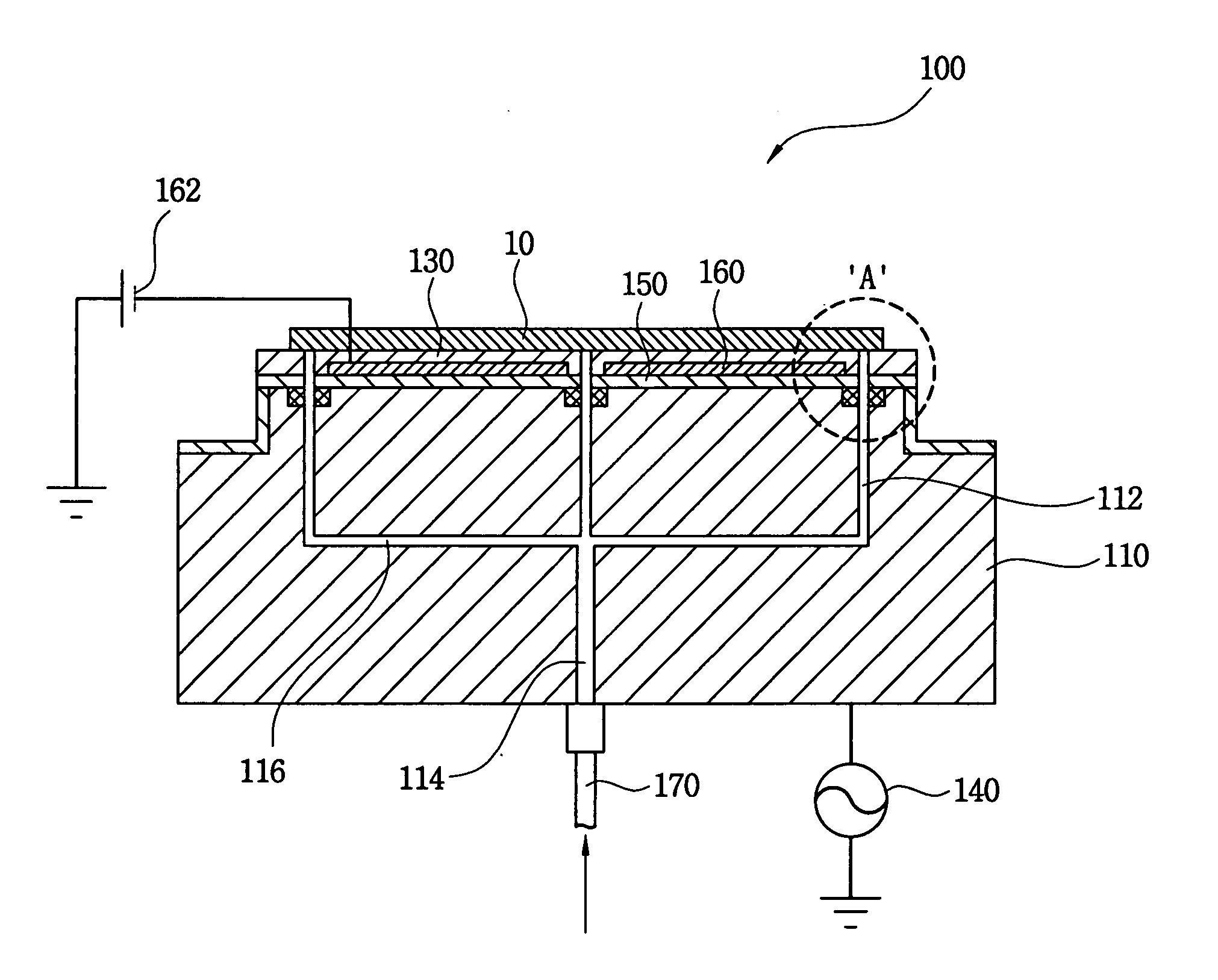
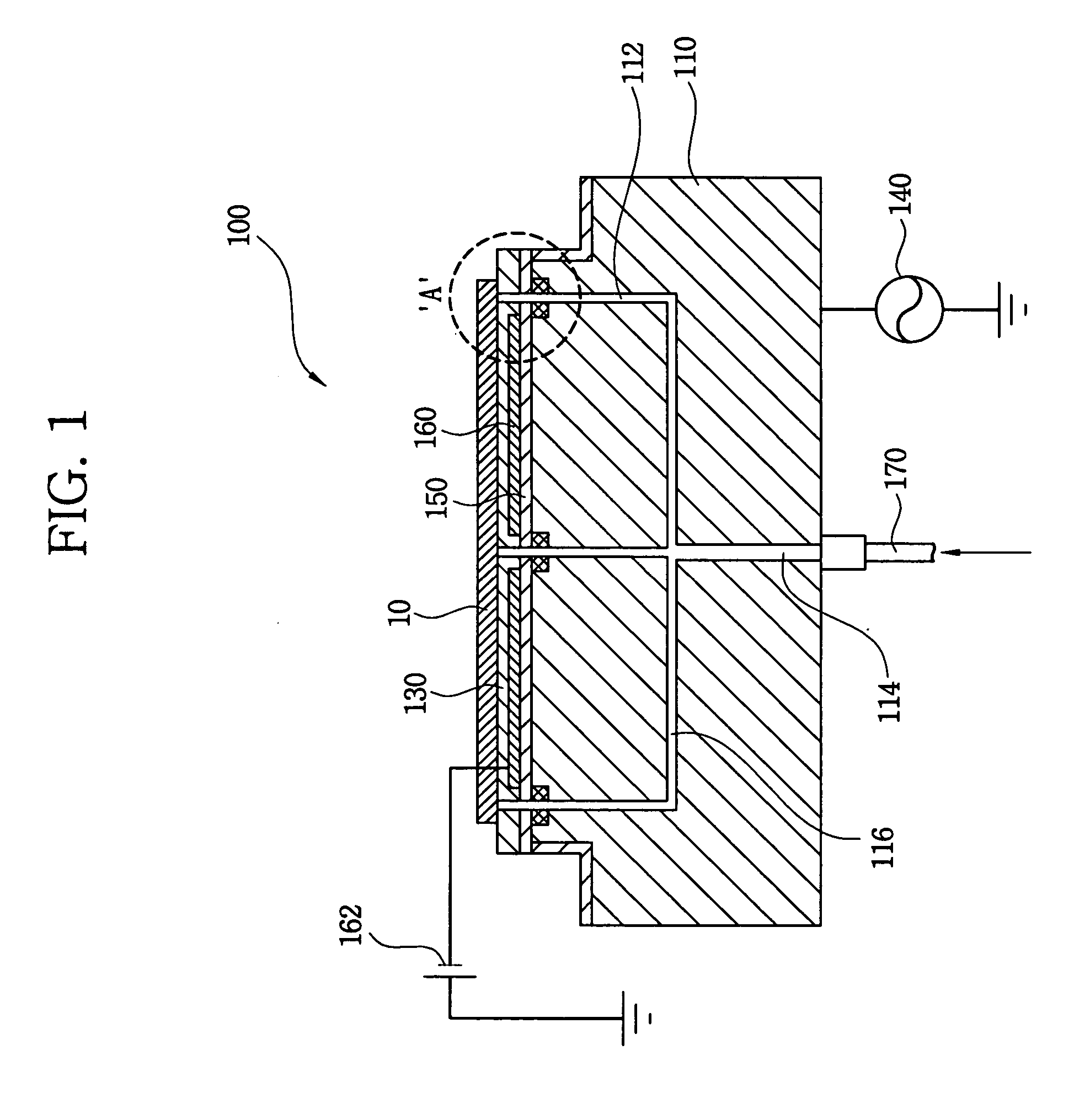
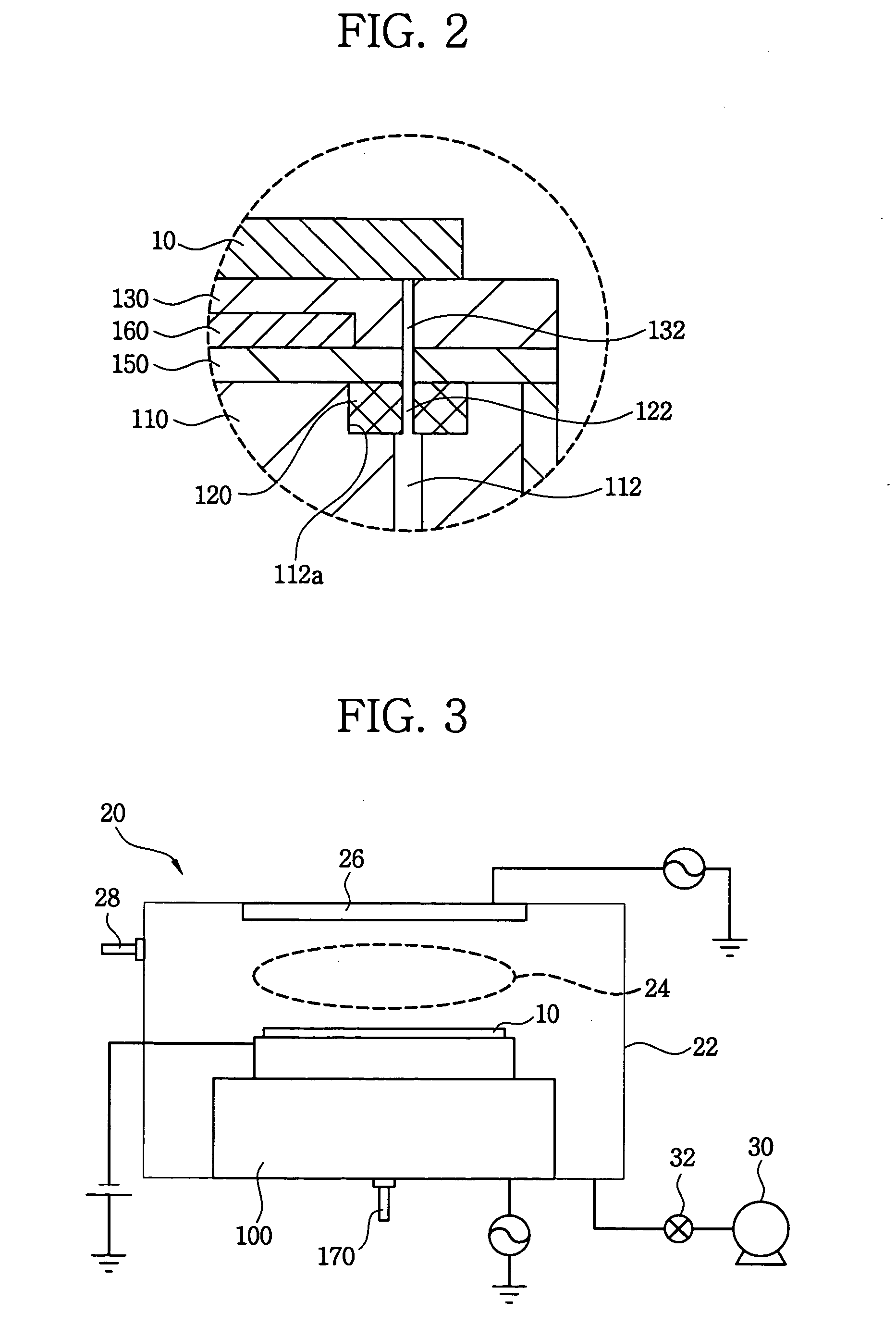
[0026]FIG. 1 is a schematic cross-sectional view showing an electrostatic chuck according to an exemplary embodiment of the present invention. FIG. 2 is an enlarged cross-sectional view of the portion “A” show...


PUM


Abstract

An electrostatic chuck to minimize an arc and a glow discharge during processing of a semiconductor substrate is provided, In one aspect, an electrostatic chuckin a processing chamber includes a body having a first hole for providing a cooling gas to a backside of a substrate to control a temperature of the substrate, an inner electrode for generating an electrostatic force and a dielectric layer. A ceramic block is tightly inserted into a first hole and has a second hole connected to the first hole. A third hole formed through the dielectric layer is connected to the first hole and the second hole. The cooling gas is provided to the backside of the substrate through the first hole or the second hole. Since the first hole is covered with the ceramic block, the generation of an arc or a glow discharge inside the first hole may be minimized, thereby preventing damage to the electrostatic chuck and improving production yields.

Description

CROSS REFERENCE TO RELATED APPLICATION [0001] This application claims priority to Korean Patent Application No. 2003-80901, filed on Nov. 17, 2003, which is incorporated herein by reference in its entirety. BACKGROUND OF THE INVENTION [0002] 1. Field of the Invention [0003] The present invention relates, generally, to an electrostatic chuck. More particularly, the present invention relates to an electrostatic chuck that minimizes the generation of an arc and / or a glow discharge during processing of a semiconductor substrate disposed in a processing chamber. [0004] 2. Description of the Related Art [0005] Generally, semiconductor devices are manufactured through a fabricating process for forming an electrical circuit on a substrate such as a silicon wafer, an electrical die sorting (EDS) process for testing electrical characteristics of the semiconductor device after the fabricating process and a package process for packaging the semiconductor devices using an epoxy resin after separ...

Claims


Application Information

Patent Timeline
IPC IPC(8): H01L21/683H01L21/306H02H1/00
CPCH01L21/6833H01L21/306
Inventor LEE, TAE-WONCHOI, JEONG-MINBAE, DO-IN
Owner SAMSUNG ELECTRONICS CO LTD
Why Eureka
Try Eureka