Optical waveguide, light source module, and optical information processing apparatus

a technology of light source module and optical information processing apparatus, which is applied in the direction of optical waveguide light guide, optical light guide, instrument, etc., can solve the problems of increasing the diameter of the beam which should be a point light source, difficult to recognize, and difficulty in electric signal wiring to increase the signal speed and density of electric signal wirings

Inactive Publication Date: 2005-05-19
SONY CORP
View PDF7 Cites 22 Cited by
  • Summary
  • Abstract
  • Description
  • Claims
  • Application Information

AI Technical Summary

Benefits of technology

[0049] The present invention is advantageously applicable to a display configured so that a predetermined flux of light can efficiently be condensed by the optical waveguide and can be emitted therefrom, or so that a signal light efficiently introduced into the optical waveguide and emitted therefrom is further scan

Problems solved by technology

It is, however, difficult for electric signal wirings to increase the signal speed and density of the electric signal wirings, due to problems in occurrence of signal delay or generation of noise ascribable to time constant of the wirings.
The emitted light from the core layer 106 is therefore undesirably mixed with the emitted light from the cladding layers 102, 105, and makes it difficult to recognize the clear emitted light from the core layer 106, and this results in increase in diameter of the beam which should be a point light source, and makes it unacceptable for use in optical communica

Method used


Image

  • Optical waveguide, light source module, and optical information processing apparatus
  • Optical waveguide, light source module, and optical information processing apparatus
  • Optical waveguide, light source module, and optical information processing apparatus

Examples


first embodiment

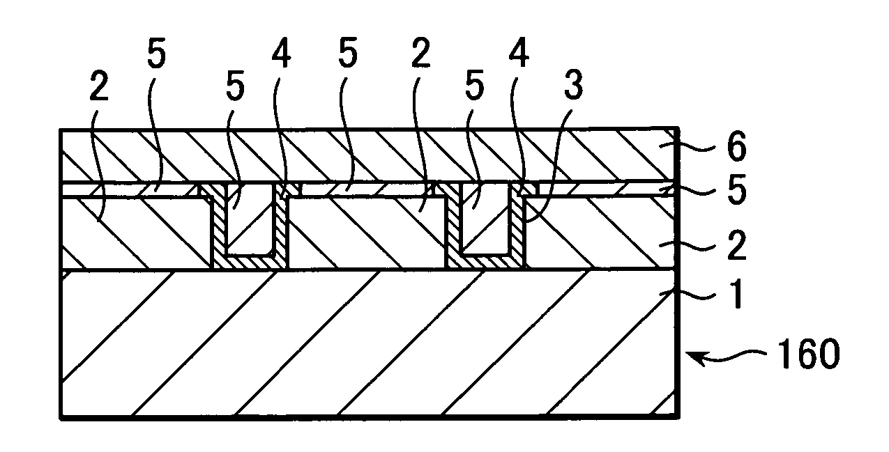
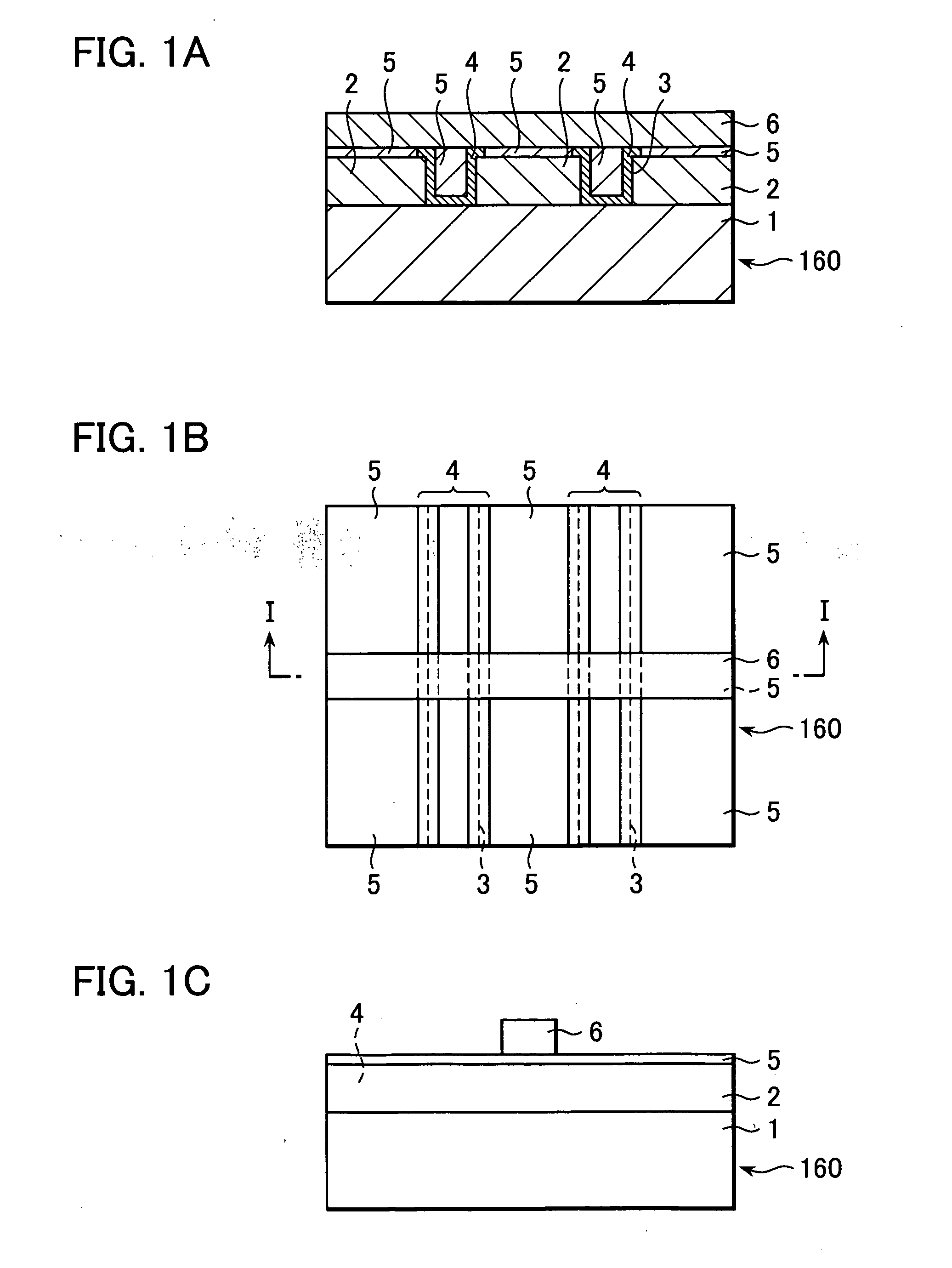
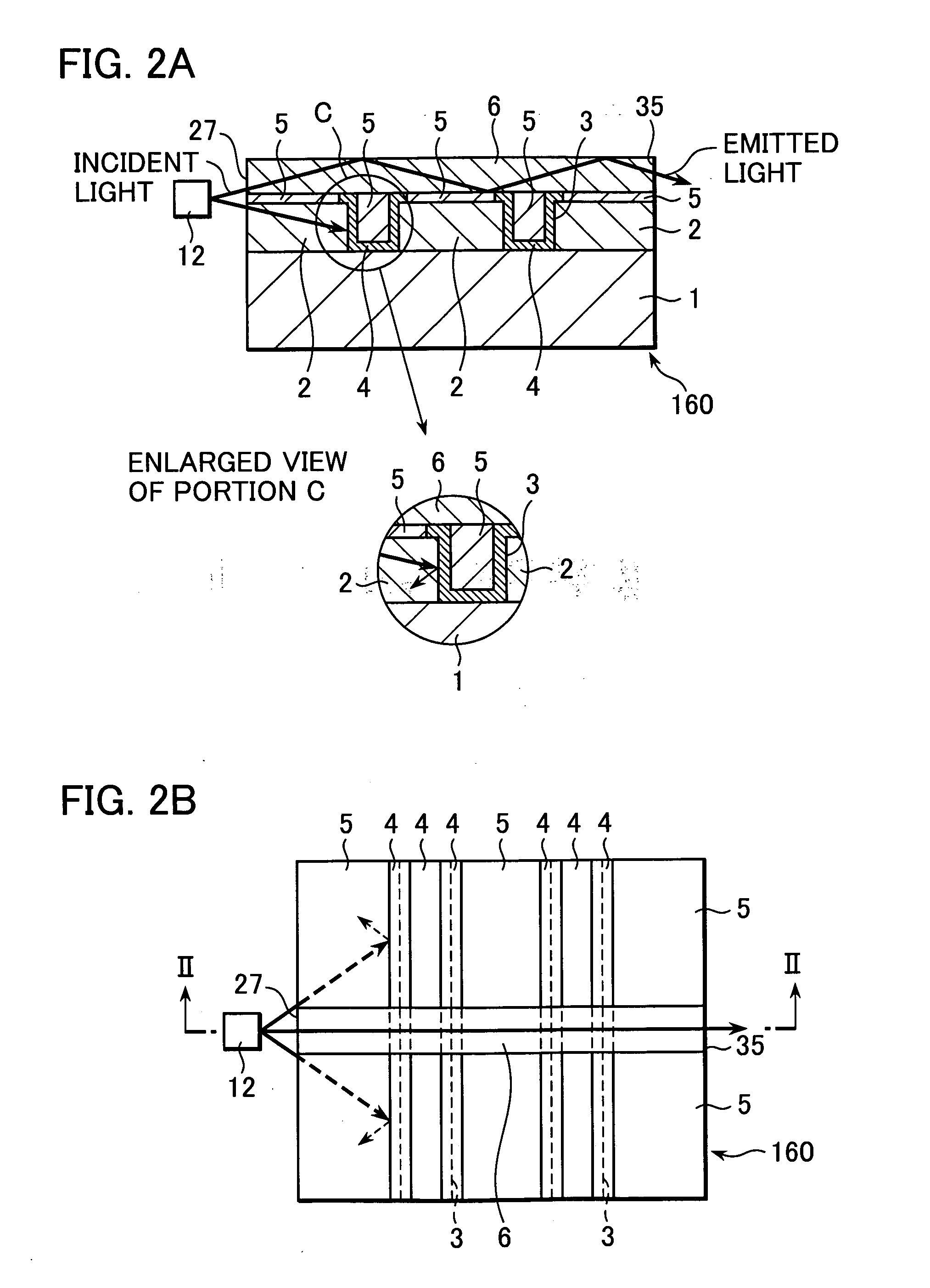
[0092] An optical waveguide of the present embodiment is configured, as shown in FIG. 1A as a sectional view taken along line I-I in a plan view of an optical waveguide 160, in FIG. 1B as a plan view, and in FIG. 1C as a side elevation, so that the a cladding layer 2, a cladding layer 5 and a core layer 6, respectively having a predetermined thickness, are formed in this order on a substrate 1 having a predetermined thickness and geometry, and metal layers 4 are disposed at two portions which extend over groove portions 3 formed in the cladding layer 2 and towards the cladding layer 5. It is to be noted that FIG. 1A is a sectional view taken along line I-I in the plan view shown in FIG. 1B. The optical waveguide herein is of air-ridge-type having a top surface and side faces of the core layer 6 exposed to the air.

[0093] The metal layers 4 have a nearly U-shape section opened upward, typically have a thickness of several tens of micrometers, and are provided two in parallel with eac...

second embodiment

[0127] The present embodiment is similar to the above-described first embodiment, except that, in an optical waveguide 163 having the same configuration with the above-described optical waveguide 160, the end portion thereof is removed typically at an angle of inclination of 45° to thereby form an inclined surface 25, and in that the substrate 37 is composed of a material having a light transmissivity, as shown in FIG. 11 and FIG. 12.

[0128] As shown in FIGS. 11A-11B and FIGS. 12A-12C, the optical waveguide 163 is configured so that the end portion of an optical waveguide having the same structure with the optical waveguide 160 is removed at an angle of inclination of 45° to thereby form a mirror-finished inclined surface 25, so that the substrate 37 is composed of a material having a large light transmissivity, and so that the LED 12 is disposed on the lower side of the substrate 37 right under the inclined surface 25. The inclined surface 25 has portions of the cladding layer 2, t...

third embodiment

[0140] The present embodiment is similar to the above-described first embodiment, except that an optical waveguide of the present embodiment is configured as a trapezoidal optical waveguide 164 in which the width-wise geometry of the core layer 6 is narrowed from the incidence surface side towards the emission surface side straightly along the direction of propagation of light, and has straight inclined surfaces 56.

[0141] As for the present embodiment, states of introduction of light into the core layer 164 and propagation of light therethrough will be described, referring to FIG. 14. It is to be assumed now that the width of the core layer 6 on the incidence surface side is widened so as to reach both side faces of the optical waveguide 164.

[0142]FIG. 14A shows a state in which the beams of light from the individual LEDs 9R, 9G, 9B are allowed to enter the core layer 6 in the optical waveguide 164 at the same time through the incidence surface 27 and are allowed to emit from the ...


PUM


Abstract

The present invention is to provide an optical waveguide capable of allowing a desired incident light to efficiently propagate towards the light emission side and to emit therefrom, and capable of preventing unnecessary incident light from propagating, and in providing a light source module and an optical information processing apparatus using the optical waveguide. The optical waveguide comprises a bonded member of a substrate, a core layer and cladding layers, configured to introduce an incident line coming into the core layer toward a light emission side thereof. A metal layer for preventing the incident light coming into the cladding layer from propagating to the light emission side is formed in a pattern intercepting a sectional plane of light transmission of said cladding layer.

Description

CROSS REFERENCES TO RELATED APPLICATIONS [0001] The present document is based on Japanese Priority Document JP 2003-386686, filed in the Japanese Patent Office on Nov. 17, 2003, the entire contents of which being incorporated herein by reference. BACKGROUND OF THE INVENTION [0002] 1. Technical Field [0003] The present invention relates to an optical waveguide comprising a bonded member of a core layer and cladding layers, suitable for light source module, optical interconnection, optical communication and so forth, and also to an optical information processing apparatus such as display. [0004] 2. Description of Related Art [0005] Heretofore, mainly electric signals have taken part in information transmission over relatively short distances, typically between boards in a single electronic instrument, and between chips on a single board, in which further increase in signal speed and in density of signal wirings will be necessary in order to upgrade performances of integrated circuits....

Claims


Application Information

Patent Timeline
IPC IPC(8): G02B6/122G02B6/42G02B6/14
CPCG02B6/122G02B6/42G02B6/14
Inventor ARAKIDA, TAKAHIRO
Owner SONY CORP
Why Eureka
Try Eureka