
Substrate and method for producing a substrate

a substrate and substrate technology, applied in the direction of basic electric elements, electrical apparatus, semiconductor devices, etc., can solve the problems of deterioration of the electrical properties of mos transistors, insufficient volume for forming pocket regions in thin-film soi technology, and inability to meet the requirements of substrate production,

Inactive Publication Date: 2005-05-26
INFINEON TECH AG
View PDF9 Cites 8 Cited by
  • Summary
  • Abstract
  • Description
  • Claims
  • Application Information

AI Technical Summary

Benefits of technology

[0029] The invention is based on the problem of providing a substrate in which the above-described disadvantages during wiring or during exposure of the substrate are avoided.

Problems solved by technology

A central problem of conventional integrated circuits is the deterioration in the electrical properties of MOS transistors with increasing structural fineness on account of effects such as the punch-through effect and the latch-up effect.
However, technological problems exist on the one hand in producing an insulated monocrystalline layer on a silicon oxide layer and on the other hand in integrating this process step into an overall process in the production of an integrated circuit.
However, for technological reasons, the material for the gate region may be predetermined or the free material selection may be restricted, so that the material selection as a parameter for setting the threshold voltage of a field-effect transistor may be obviated.
Furthermore, in SOI technology, usually a very thin silicon layer is provided above the silicon oxide layer, so that clearly a sufficient volume does not remain for forming pocket regions in thin-film SOI technology.
Furthermore, setting the threshold voltage by doping the channel region has the disadvantage that, on account of technologically unavoidable inhomogeneity fluctuations in the charge carrier density in the channel region of different field-effect transistors of a circuit, the threshold voltage may also be subjected to fluctuation in an undesirable manner.
Furthermore, the doping of the channel region leads to an increase in the number of scattering centers for charge carriers and therefore results in an undesirable increase in the nonreactive resistance.
However, the free selection of a material of the gate region may be restricted for technological reasons.
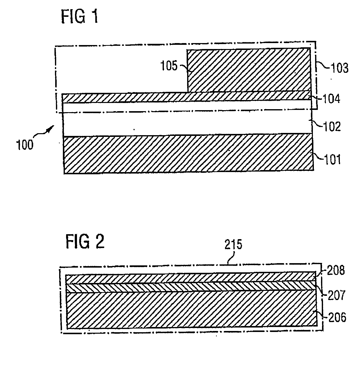
This method for producing a mixed substrate in accordance with the prior art gives rise to problems in the further processing of the mixed substrate as a result of the regions of different thickness 104 and 105.
The steps caused by the different thicknesses of the silicon layers constitute a problem in the case of a subsequent gate wiring across the boundaries of the different FD regions and PD regions.
A further problem is that, during the subsequent lithographic exposure of the surface, as a result of the limited focus depth of a stepper used for the exposure, problems can arise during the exposure across the boundaries present between in each case a PD region and an FD region.
Furthermore, the methods in which the semiconductor layer is etched back in regions or in which the semiconductor layer is oxidized exhibit the problem that it is difficult to exactly control the silicon thicknesses produced by means of the etching or oxidation.

Method used


Image

  • Substrate and method for producing a substrate
  • Substrate and method for producing a substrate
  • Substrate and method for producing a substrate

Examples


Embodiment Construction

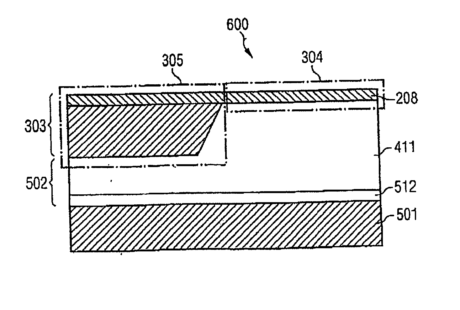
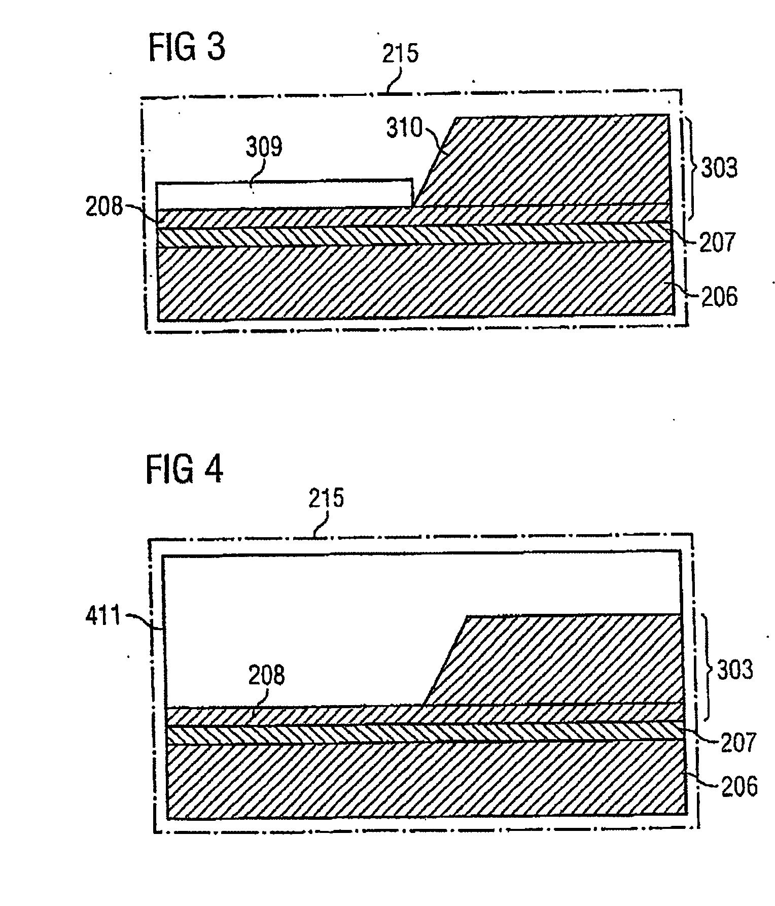
[0098]FIG. 2 shows an auxiliary carrier substrate 215 having an auxiliary carrier layer 206 made of silicon. A layer 207 made of porous silicon is applied on the auxiliary carrier layer 206 made of silicon. A thin first semiconductor partial layer 208 made of silicon is applied on the layer 207 made of porous silicon. The thin first semiconductor partial layer 208 has a thickness in the range of 5 nm to 30 nm. The thickness of the thin first semiconductor layer 208 is preferably 20 nm.

[0099]FIG. 3 shows the auxiliary carrier substrate 215 after further method steps, a protective layer 309 made of silicon oxide being applied on the thin first semiconductor partial layer 208. Said protective layer 309 is converted, i.e. patterned, into a masking layer by means of etching back the silicon oxide in partial regions of the auxiliary carrier substrate 215. In a further process step, after the removal of a resist layer, applied for the etching-back, in the regions of the thin first semicon...


PUM


Abstract

Substrate having a first partial substrate with a carrier layer and a second partial substrate, which is bonded to the first partial substrate. The second partial substrate has an insulator layer, which is applied on the carrier layer and has at least two regions each having a different thickness, thereby forming a stepped surface of the insulator layer, and a semiconductor layer, which is applied to the stepped surface of the insulator layer and is formed at least partially epitaxially, wherein the semiconductor layer has a planar surface which is opposite to the stepped surface of the insulator layer. Transistors are formed on the semiconductor layer.

Description

CROSS-REFERENCE TO RELATED APPLICATION [0001] This application is a continuation of International Patent Application Serial No. PCT / DE03 / 01281, filed Apr. 16, 2003, which published in German on Oct. 23, 2003 as WO 03 / 088310, and is incorporated herein by reference in its entirety.FIELD OF THE INVENTION [0002] The invention relates to a substrate and a method for producing a substrate. BACKGROUND OF THE INVENTION [0003] Field-effect transistors are employed in many areas of electronics, in particular as switch elements or as storage elements of an integrated circuit. [0004] New types of transistors are being developed and used particularly in the course of the ever increasing requirements made of mass storage devices. [0005] In order to increase the storage density of a semiconductor memory, Eitan, B, Pavan, P, Bloom, I, Aloni, E, Frommer, A, Fiñzi, D (2000) “NROM: A Novel Localized Trapping, 2-Bit Nonvolatile Memory Cell” IEEE Electron Device Letters 21(11): 543-545, discloses using...

Claims


Application Information

Patent Timeline
Patent Type & Authority Applications(United States)
IPC IPC(8): H01L21/20H01L21/762H01L27/01
CPCH01L21/76254
Inventor HOFMANN, FRANZLUYKEN, RICHARD JOHANNESROESNER, WOLFGANGSPECHT, MICHAELSTADELE, MARTIN
Owner INFINEON TECH AG
Learn More