Low coefficient of thermal expansion (CTE) semiconductor packaging materials

a technology of thermal expansion and semiconductor packaging, applied in semiconductor devices, semiconductor/solid-state device details, electrical devices, etc., can solve the problems of tensile force cracking, ripping or otherwise damaging sensitive features or components on or near the surface, and the interface of the two materials may be subject to high stress. , the effect of reducing the tensile for

Inactive Publication Date: 2005-05-26
TEXAS INSTR INC
View PDF10 Cites 49 Cited by
  • Summary
  • Abstract
  • Description
  • Claims
  • Application Information

AI Technical Summary

Benefits of technology

[0004] Disclosed is a low-CTE packaging material for assembling a semiconductor die into a package and a method for assembling a semiconductor die into a package, in which the packaging material comprises a negative-CTE material. A low-CTE packaging material in accordance with the embodiment...

Problems solved by technology

Since the material of a semiconductor wafer—commonly silicon—tends to be relatively fragile and brittle, dies are often assembled into a protective housing, or package, before they are interconnected with a printed circuit board (PCB).
When a relativel...

Method used


Image

  • Low coefficient of thermal expansion (CTE) semiconductor packaging materials
  • Low coefficient of thermal expansion (CTE) semiconductor packaging materials
  • Low coefficient of thermal expansion (CTE) semiconductor packaging materials

Examples


Embodiment Construction

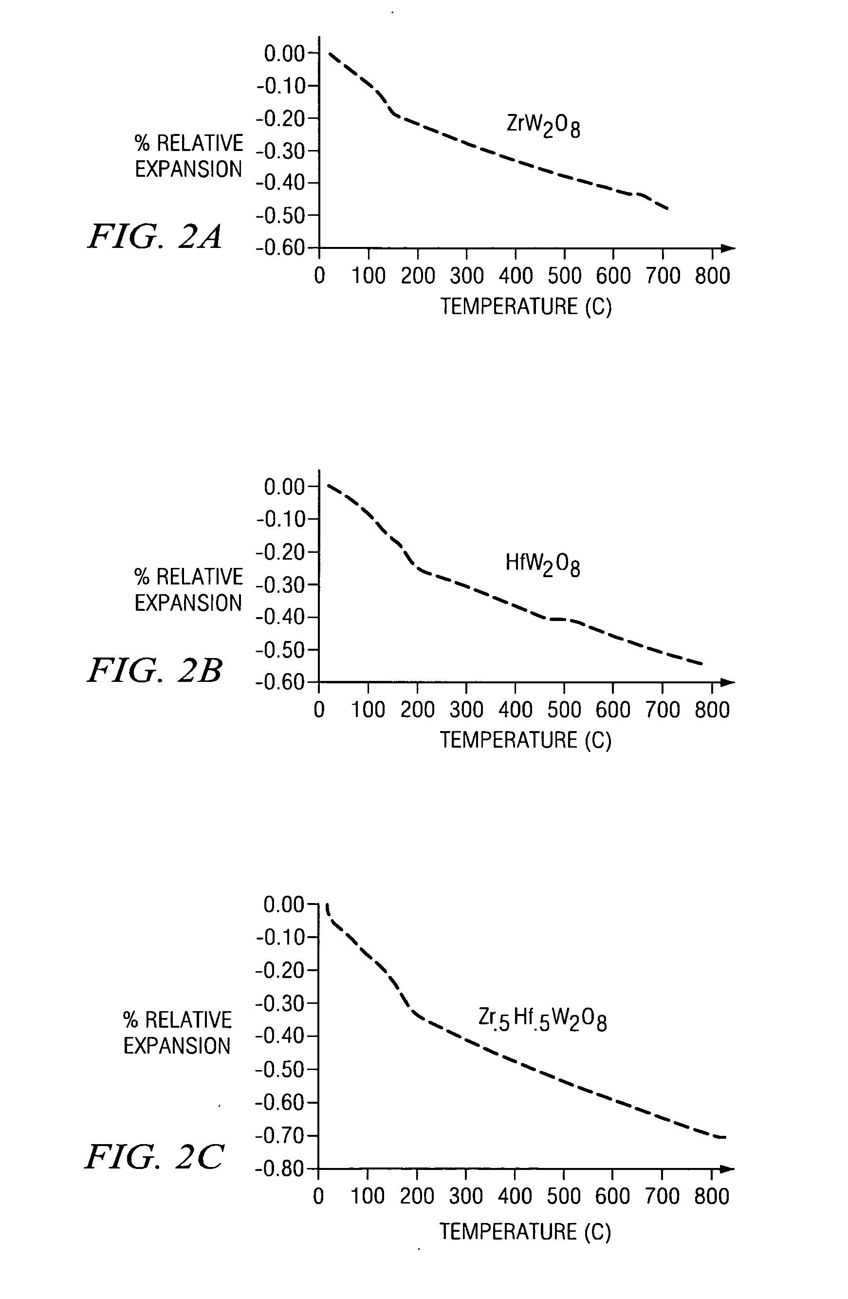
[0015] Zirconium tungstate (ZrW2O8) is a relatively new material having a negative CTE. That is, zirconium tungstate tends to shrink, rather than expand, when heated. If mixed with a typical positive-CTE material to form a composite material, a negative-CTE material such as zirconium tungstate may be able to counteract expansion of the positive-CTE material to form a composite material with little or no thermal expansion. Further, by varying the amount of negative-CTE material introduced into a mixture with the positive-CTE material, the CTE of the composite may be designed to approach a specific value, such as that of a silicon die (e.g., about 3 ppm / C) or another adjacent material.

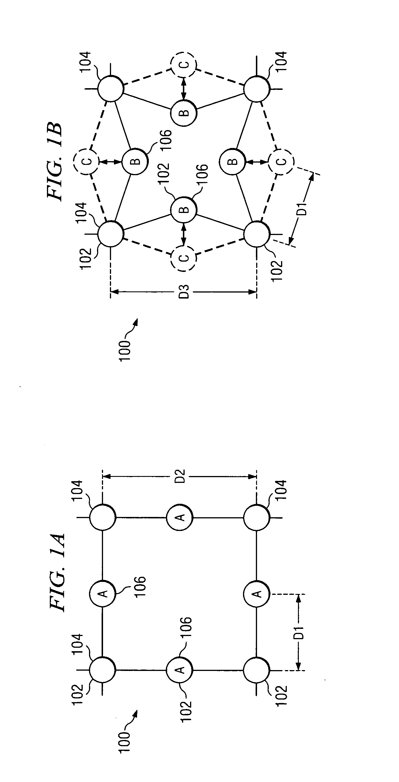
[0016] Referring now to FIG. 1A, a simplified molecular lattice structure 100 is shown of a negative-CTE material prior to thermal excitement. In the configuration shown, each atom 102 is at a distance D1 from each adjacent atom on the lattice 100. Each corner atom 104 has a distance D2 from adjacent co...


PUM


Abstract

A low-CTE packaging material for assembling a semiconductor die into a package and a method for assembling a semiconductor die into a package, in which the packaging material comprises a negative-CTE material. The low-CTE packaging material in accordance with the embodiments of the invention may be a die attach material, a lid attach material, or an encapsulant, such as a mold compound or glob-top material. Preferably, the negative-CTE material is a tungstate compound, such as zirconium tungstate, halfnium tungstate or a solution of zirconium and halfnium tungstate.

Description

BACKGROUND OF THE INVENTION [0001] Integrated circuits are fabricated on the surface of a semiconductor wafer in layers and later singulated into individual dies. Since the material of a semiconductor wafer—commonly silicon—tends to be relatively fragile and brittle, dies are often assembled into a protective housing, or package, before they are interconnected with a printed circuit board (PCB). These assembled dies and their surrounding packages may be referred to as “packaged semiconductor devices.”[0002] A concern in packaging technology is the respective coefficients of thermal expansion (CTE) of adjacent materials within a package. A CTE is a physical value that denotes the tendency of a material to expand in relation to temperature increases. As shown in Table 1 below, a silicon die may have a CTE of about 3 ppm / C, while surrounding packaging materials may have significantly higher CTE values. Exemplary values for an encapsulant are represented for encapsulants below their res...

Claims


Application Information

Patent Timeline
IPC IPC(8): H01L23/06H01L23/29H01L23/31
CPCH01L23/06H01L24/48H01L23/3128H01L2224/16225H01L2224/32225H01L2224/48091H01L2224/48227H01L2224/48228H01L2224/73204H01L2224/73253H01L2224/73265H01L2924/15311H01L2924/16152H01L23/295H01L2924/10253H01L2924/00014H01L2924/00H01L2924/14H01L2924/181H01L2924/00012H01L2224/45099H01L2224/45015H01L2924/207
Inventor CHUANG, SHIH-FANG
Owner TEXAS INSTR INC
Why Eureka
Try Eureka