Disconnection and short detecting circuit that can detect disconnection and short of a signal line transmitting a differential clock signal
- Summary
- Abstract
- Description
- Claims
- Application Information
AI Technical Summary
Benefits of technology
Problems solved by technology
Method used
Image
Examples
first preferred embodiment
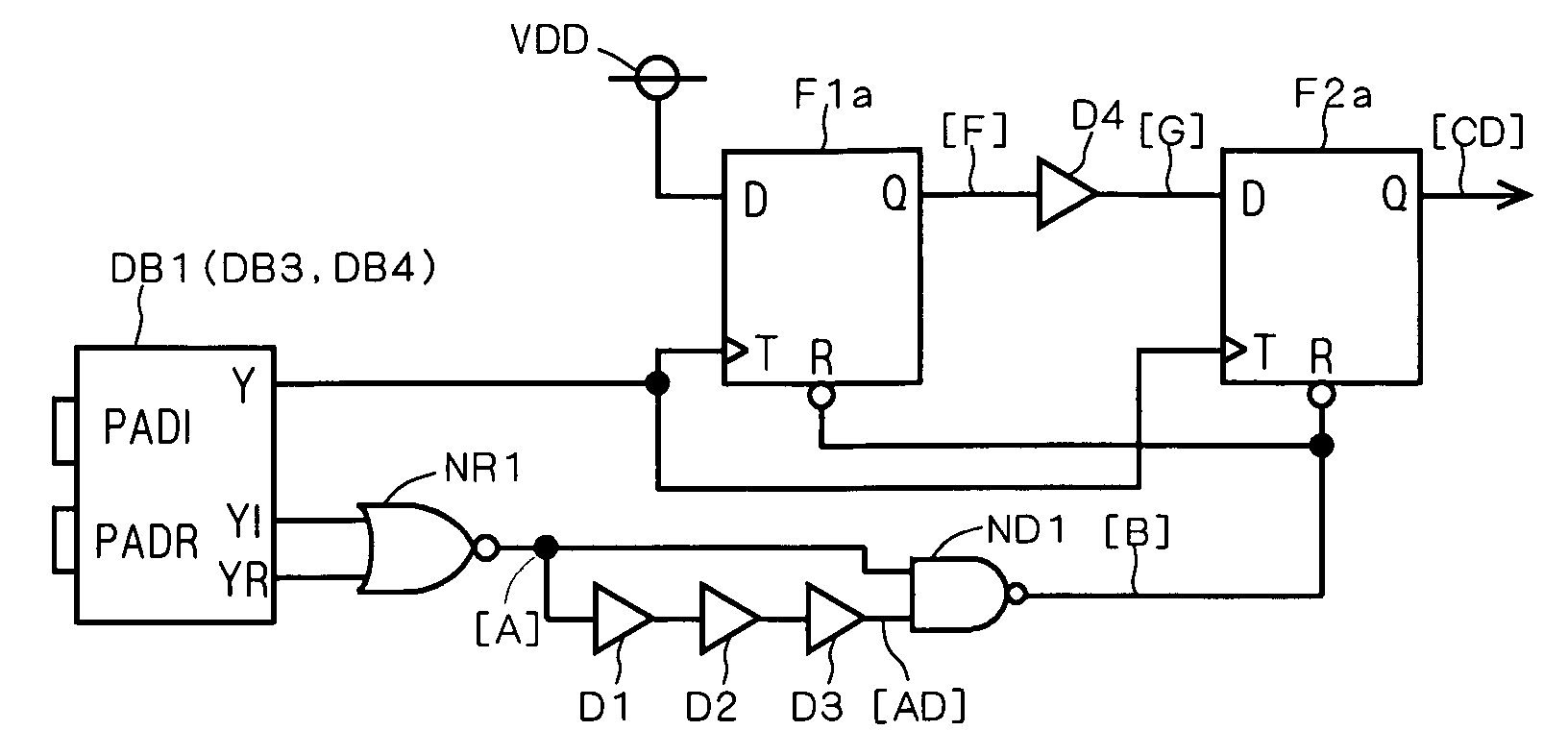
[0067] A first preferred embodiment is directed to a disconnection and short detecting circuit that more reliably detects disconnection and short of a signal line transmitting a differential clock signal by disposing a plurality of comparators and so as to compare a non-inverting clock signal and an inverting clock signal with a potential unaffected by a terminating resistor.
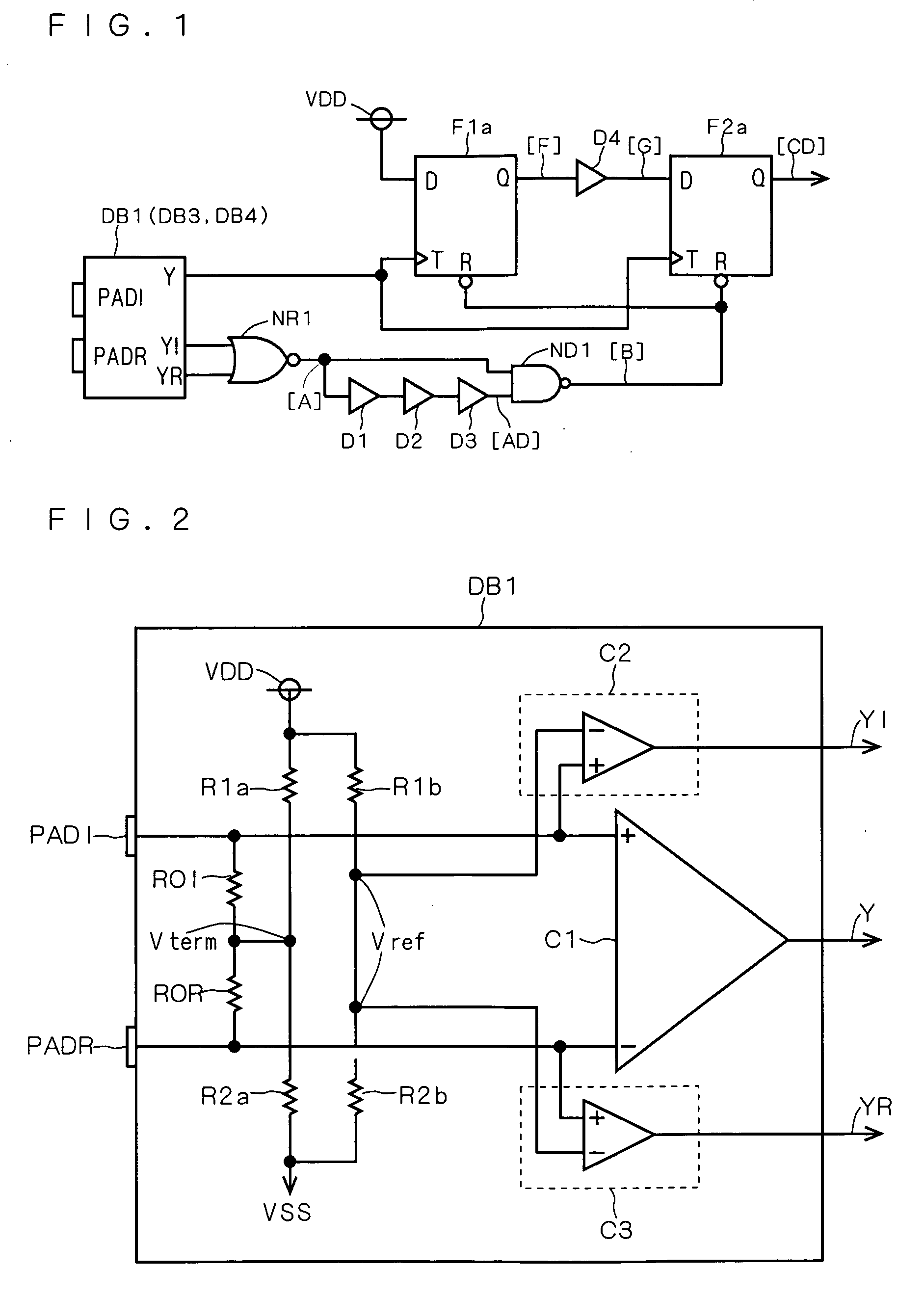
[0068]FIG. 1 is a diagram showing a disconnection and short detecting circuit of the first preferred embodiment. This circuit has a differential buffer part DB1, as shown in FIG. 1.
[0069]FIG. 2 is a diagram showing a detailed configuration of the differential buffer part DB1. As shown in FIG. 2, the differential buffer part DB1 has a first clock input end PADI to which a non-inverting clock signal is inputted, and a second clock input end PADR to which inputted is an inverting clock signal, the phase of which is the reverse of that of the non-inverting clock.
[0070] One end of a first terminating resistor R0I ...
second preferred embodiment
[0118] A second preferred embodiment is a modification of the disconnection and short detecting circuit of the first preferred embodiment. Specifically, first and second D-flip-flop circuits with set function are employed in place of the first and the second D-flip-flop circuit F1a and F2a with reset function in the first preferred embodiment.
[0119]FIG. 6 is a diagram showing a disconnection and short detecting circuit in accordance with the second preferred embodiment. The device configuration in FIG. 6 is the same as that in FIGS. 1 and 2, except that the first and the second D-flip-flop circuits F1b and F2b with set function are disposed in place of the first and the second D-flip-flop circuits F1a and F2a with reset function in FIG. 1; that the signal [B] from the two-input NAND circuit ND1 is inputted to set terminals S of the first and the second D-flip-flop circuits F1b and F2b; that instead of a power supply potential VDD, a grounding potential VSS is inputted to an input e...
third preferred embodiment
[0122] A third preferred embodiment is also a modification of the disconnection and short detecting circuit of the first preferred embodiment. Specifically, the delay circuit D4 between the first and the second D-flip-flop circuits F1a and F2a of the first preferred embodiment is eliminated, and it is configured so as to invert and input a signal Y to the second D-flip-flop circuit F2a.
[0123]FIG. 7 is a diagram showing a disconnection and short detecting circuit in accordance with the third preferred embodiment. The device configuration is the same as that in FIGS. 1 and 2, except that instead of the delay circuit D4, an inverter IV1 is disposed so as to invert and input the signal Y to the second D-flip-flop F2a.
[0124] With this configuration, the first D-flip-flop circuit F1a asserts and outputs, as a signal [G], a power supply voltage VDD by the rise transition from Low to Hi of the signal Y received at a clock input end T, for example.
[0125] On the other hand, the second D-fl...
PUM
 Abstract
Description
Claims
Application Information


