Two-modulus prescaler circuit

a prescaler circuit and two-modulus technology, applied in the direction of pulse technique, radiation controlled device, semiconductor device, etc., can solve the problem of difficulty in and achieve the effect of reducing power supply voltage and signal amplitud

a prescaler circuit and two-modulus technology, applied in the direction of pulse technique, radiation controlled device, semiconductor device, etc., can solve the problem of difficulty in and achieve the effect of reducing power supply voltage and signal amplitud

US20050116258A1Inactive Publication Date: 2005-06-02NIPPON TELEGRAPH & TELEPHONE CORP +1

Image

  • Two-modulus prescaler circuit
  • Two-modulus prescaler circuit
  • Two-modulus prescaler circuit

Examples


first embodiment

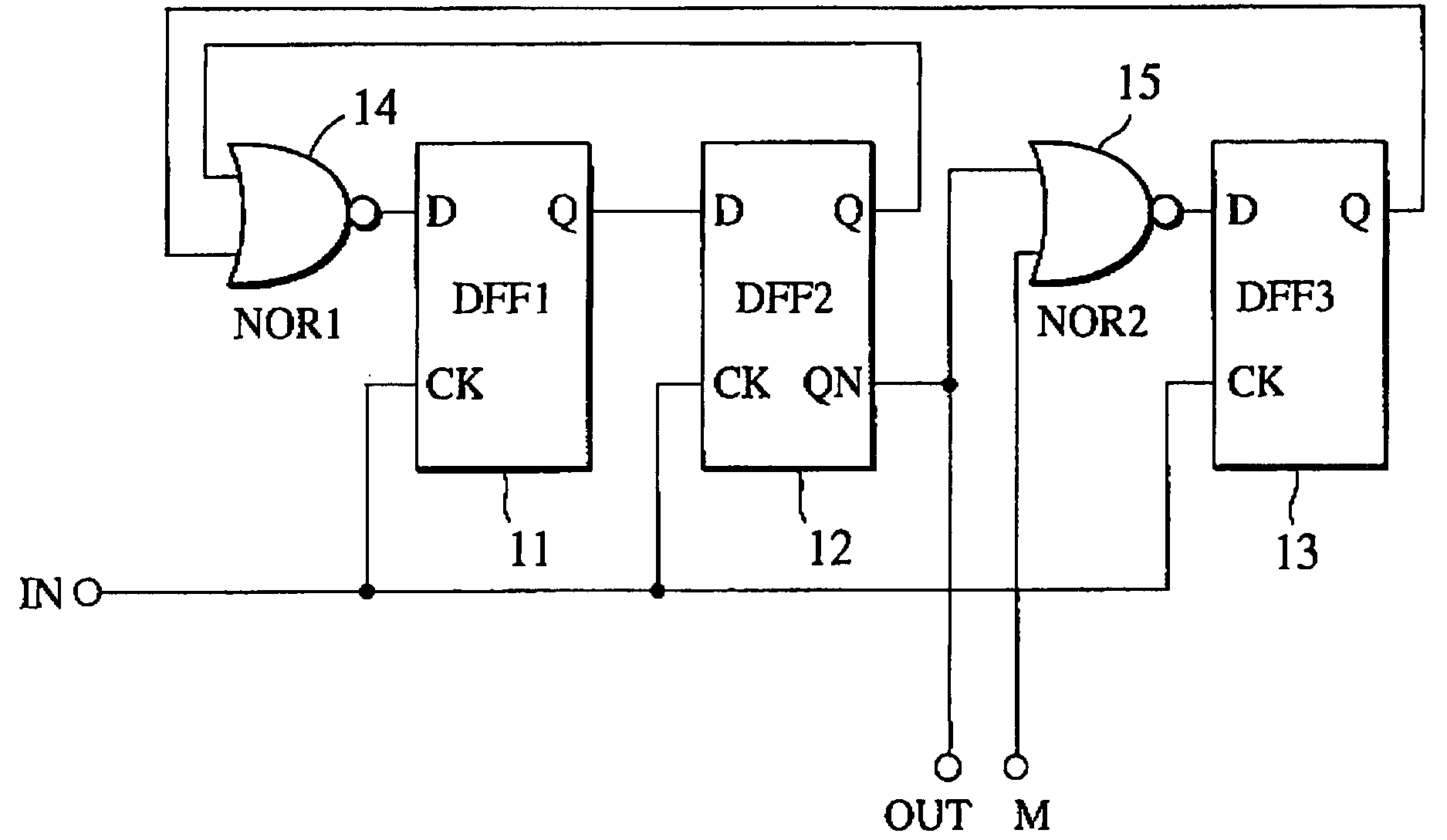
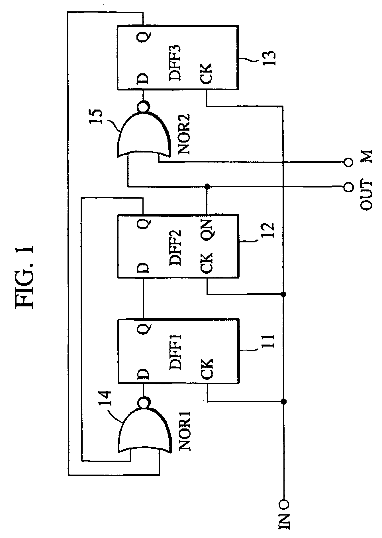
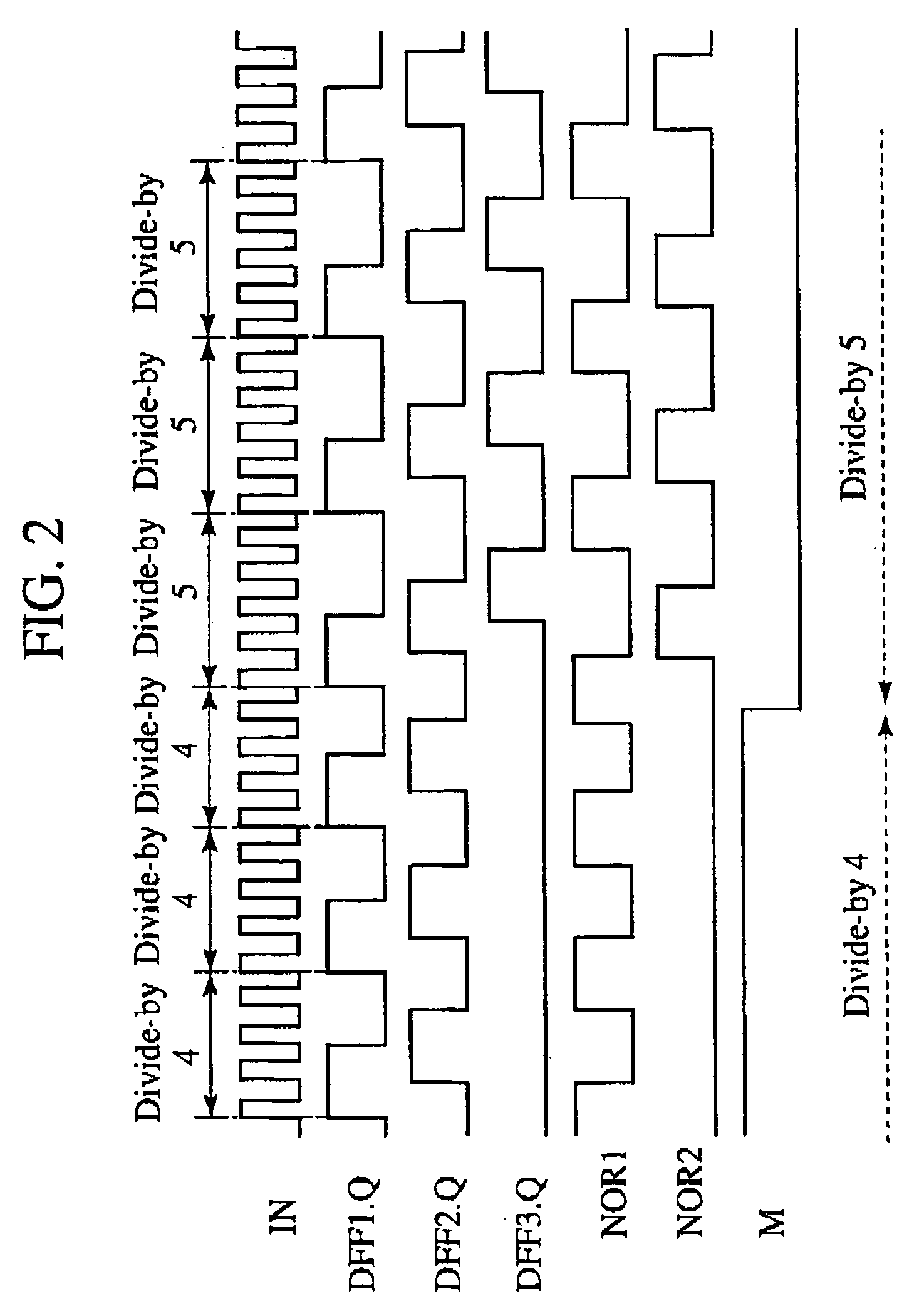
[0027]FIG. 6 is a view showing the present invention. This embodiment corresponds to an aspect of the present invention according to claim 1. In the drawing, reference numerals 1 to 3 denote DFF circuits, and 4 and 5 denote NOR circuits. The circuit of FIG. 6 is configured so that differential signals are inputted to / outputted from all the DFF circuits (D flip-flop circuits) and NOR circuits (multi-input logical gate circuits). An example of the differential input / output NOR circuit is shown in FIG. 7. This circuit corresponds to a NOR circuit defined by another aspect of the present invention according to claim 2.

[0028] The circuit of FIG. 7 is a NOR circuit operated in a current mode in order to ensure high speed performance. In FIG. 7, R1 and R2 denote resistors: M1 to M4, transistors; I-1, a current source; AP, an input signal; and YP, an output signal. When the terminals AP and BP in the circuit of FIG. 7 are Hi, AN and BN are Low. At this time, current flows through R1 but doe...

second embodiment

[0032]FIG. 8 is a view showing the present invention, corresponding to still another aspect of the invention according to claim 3. The circuit of FIG. 8 is a circuit in which the transistor M2 of the DFF circuit with a NOR gate shown in FIG. 5 is replaced with transistors M2A and M2B which are connected in series. In the circuit of FIG. 8, differential signals are applied between AP and AN and between BP and BN.

[0033] In reading data when CP is Low, only in the case where AP and BP are Low, AN and BN are Hi, and current flows through R2. Accordingly, Hi is read. In other cases, current flows through any one or both of M1A and M1B, and any one or both of M2A and M2B are turned off. Accordingly, current flows through R1, and Low is read.

[0034] Therefore, the circuit of FIG. 8 operates as the DFF circuit with a NOR gate. It is possible to implement the fully differential “divide-by 4 / divide-by 5 divider” by applying the DFF circuit with a NOR gate of FIG. 8 to each of combinations of ...


PUM


Abstract

In the dual modulus prescaler circuit, an output terminal of the first multi-input logic gate circuit is connected to a data input terminal of a first D flip-flop circuit; output terminals of the first to (n-2)th D flip-flop circuits are, respectively, connected to data input terminals of the second to (n-1)th D flip-flop circuits; output terminals of the (n-1)th and nth D flip-flop circuits are connected to input terminals of the first multi-input logic gate circuit; the second multi-input logic gate circuit is connected to the output terminal of the (n-1)th D flip-flop circuit and receives a switching signal; and an output terminal of the second multi-input logic gate circuit is connected to a data input terminal of the nth D flip-flop circuit. Moreover, all the aforementioned connections are connections using differential signals.

Description

TECHNICAL FIELD [0001] The present invention relates to a dual modulus prescaler circuit applicable to frequency synthesizers and the like. Specifically, the present invention relates to a dual modulus prescaler circuit which can operate with small signal amplitude and with reduced power consumption. BACKGROUND OF THE INVENTION [0002] A “divide-by 4 / divide-by 5 divider” switchable between divide-by 4 and divide-by 5 modes, which is a basis for a dual modulus prescaler used for a pulse swallow type PLL synthesizer, is composed of a circuit as shown in FIG. 1. In FIG. 1, reference numerals 11 to 13 denote D flip-flop circuits (DFF circuits), and reference numerals 14 and 15 denote NOR circuits. This circuit is configured to switch between divide-by 4 and divide-by 5 modes by means of a polarity of an input signal of a terminal M. [0003]FIG. 2 is a timing chart showing an operation of the “divide-by 4 / divide-by 5 divider”. As shown in FIG. 2, in the “divide-by 4 / divide-by 5 divider”, w...

Claims


Application Information

Patent Timeline
02 Jun 2005
Publication
US20050116258A1
IPC
H03K21/00; H03K23/64; H03K23/66
CPC
H03K23/667
Inventors
YAMAGISHI, AKIHIRO; TSUKAHARA, TSUNEO