Organic electroluminescent device and organic compound for use in organic electroluminescent device

a technology of which is applied in the field organic compounds, can solve the problems that the improvement of organic electroluminescent devices is not specifically investigated, and achieve the effect of high reliability and high luminous efficiency

Active Publication Date: 2005-06-02
SANYO ELECTRIC CO LTD
View PDF3 Cites 20 Cited by
  • Summary
  • Abstract
  • Description
  • Claims
  • Application Information

AI Technical Summary

Benefits of technology

[0008] It is an object of the invention to provide an organic electroluminescent device comprising a blue light-emitting layer which can have high luminous efficiency and high reliability and to provide an organic compound which can be used as a blue light-emitting material for such an organic electroluminescent device.

Problems solved by technology

However, such improvements are not specifically investigated for organic electroluminescent devices having a blue light-emitting layer.

Method used


Image

  • Organic electroluminescent device and organic compound for use in organic electroluminescent device
  • Organic electroluminescent device and organic compound for use in organic electroluminescent device
  • Organic electroluminescent device and organic compound for use in organic electroluminescent device

Examples


example 1

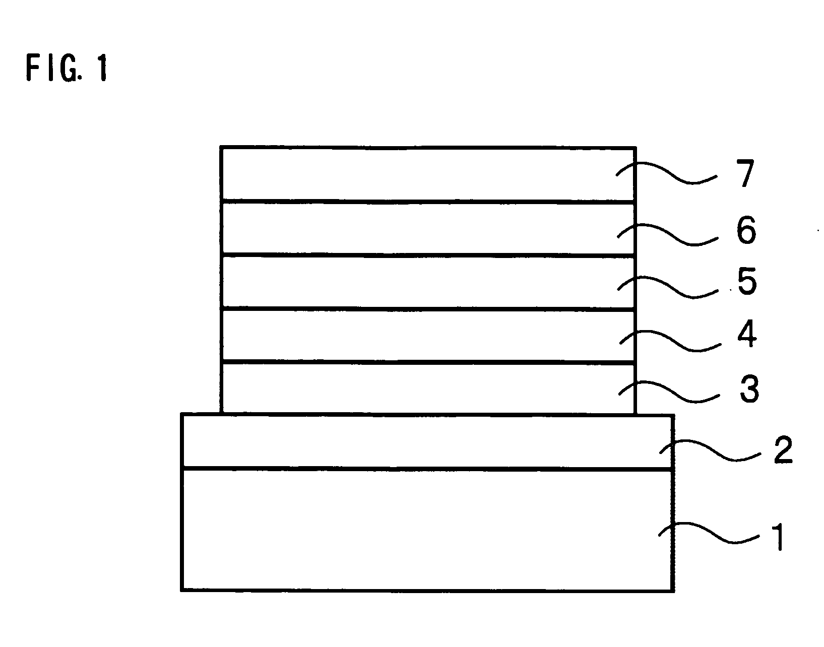
[0041] As shown in FIG. 1, a transparent hole-injecting electrode (anode) 2 made of an indium-tin compound (hereinafter referred to as ITO) was formed on a glass substrate 1, and a hole-injecting layer 3 made of CuPc (10 nm in thickness) was formed on the hole-injecting electrode 2. A hole-transporting layer 4 made of NPB (75 nm in thickness) was formed on the hole-injecting layer 3.

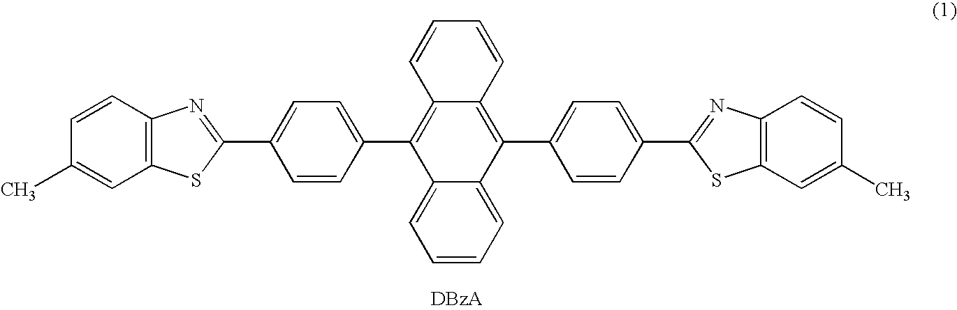
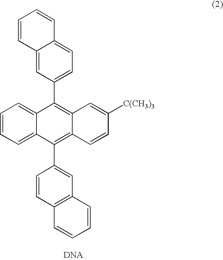
[0042] A blue light-emitting layer 5 was formed on the hole-transporting layer 4. The blue light-emitting layer 5 was made of a composition comprising a host material of DNA which contained 2.5% by weight of the luminescent dopant DBZA and 7% by weight of the assist dopant NPB.

[0043] An electron-transporting layer 6 (10 nm in thickness) made of Alq was formed on the blue light-emitting layer 5. An electron-injecting electrode (cathode) 7 composed of LiF (1 nm in thickness) and Al (200 nm in thickness) was formed on the electron-transporting layer 6.

[0044] Each layer was formed in a vacuum of 5×10⁻⁵ Pa...

example 2

[0050] As shown in Table 4, the blue light-emitting layer of this example comprises first and second blue light-emitting layers, wherein only the first blue light-emitting layer contains the assist dopant. The first blue light-emitting layer contains 7% by weight of NPB and 2.5% by weight of DBZA and has a thickness of 10 nm. The second blue light-emitting layer contains 2.5% by weight of DBZA and has a thickness of 30 nm.

TABLE 4Hole-Hole-First Blue Light-EmittingSecond Blue Light-EmittingElectron-InjectingTransportingLayerLayerTransportingCathodeLayerLayerThick-Lumi-Thick-Lumi-Layer(Thick-(Thickness:(Thickness:nessHostnescentAssistnessHostnescentAssist(Thickness:ness:Anodenm)nm)(nm)MaterialDopantDopant(nm)MaterialDopantDopantnm)nm)Ex. 2ITOCuPc(10)NPB(75)10DNAFormulaNPB30DNAFormulaAbsentAlq(10)LiF(1) / (1)(7% by(1)Al(200)DBzAweight)DBzA(2.5% by(2.5% byWeight)Weight)

[0051] The blue organic electroluminescent device of this example was evaluated for light-emitting properties as in Exa...


PUM

PropertyMeasurementUnit
luminescence peak wavelengthaaaaaaaaaa
thicknessaaaaaaaaaa
thicknessaaaaaaaaaa

Abstract

An organic electroluminescent device includes a hole-injecting electrode, an electron-injecting electrode and a blue light-emitting layer which is provided between the electrodes and contains a host material, a luminescent dopant and an assist dopant for complementing carrier transport of the host material. When the host material is an electron-transporting material, the assist dopant has a smaller absolute HOMO (Highest Occupied Molecular Orbital) energy level than the host material and a higher hole mobility than the host material.

Description

BACKGROUND OF THE INVENTION [0001] 1. Field of the Invention [0002] The invention relates to an organic electroluminescent device and an organic compound for use in such an organic electroluminescent device and particularly to an organic electroluminescent device having a blue light-emitting layer and an organic compound which can be used as a blue light-emitting material for an organic electroluminescent device. [0003] 2. Description of the Related Art [0004] Organic electroluminescent devices are a light-emitting device in which holes injected from a hole-injecting electrode and electrons injected from an electron-injecting electrode are recombined at an interface between a light-emitting layer and a carrier-transporting layer or recombined in a light-emitting layer to produce light emission. Such organic electroluminescent devices can be driven by relatively low voltage as compared with inorganic electroluminescent devices, and thus their application to flat panel displays partic...

Claims


Application Information

Patent Timeline
Patent Type & Authority Applications(United States)
IPC IPC(8): B32B9/00H01L51/50C09K11/06H01L51/00H05B33/14H05B33/22
CPCH01L51/002H01L51/0052H01L51/0058H01L51/0059H01L51/007Y10S428/917H01L51/0078H01L51/0081H01L51/5012H01L2251/308H01L51/0071H10K71/30H10K85/615H10K85/6565H10K85/631H10K85/626H10K85/657H10K85/311H10K85/324H10K50/11H10K2102/103C09K11/06
Inventor HAMADA, YUJISAITO, NOBUONISHIMURA, KAZUKIKANNO, HIROSHI
Owner SANYO ELECTRIC CO LTD
Why Eureka
Try Eureka